Ceramic substrate assembling device

A ceramic substrate and assembly device technology, which is applied in the direction of assembling printed circuits, electrical components, electrical components, etc., can solve the problems of low bonding strength, substrate susceptibility to damage, etc., to improve impact resistance, Avoid direct exposure and increase the effect of integration density

Inactive Publication Date: 2014-12-03
EAST CHINA INST OF OPTOELECTRONICS INTEGRATEDDEVICE
View PDF5 Cites 3 Cited by
  • Summary
  • Abstract
  • Description
  • Claims
  • Application Information

AI Technical Summary

Problems solved by technology

[0002] As we all know, ceramic substrates are increasingly used in electronic circuits due to their excellent electrical insulation properties and high thermal conductivity; at present, there are usually three structures for the assembly device of ceramic substrate products: 1. The bottom surface of the substrate is welded to the outside of the product. Feet, the metal frame is welded around the top surface of the substrate, and the top surface of the substrate is sealed and welded by the metal cover plate and the metal frame to realize the package. Due to the brittle characteristics of ceramic materials, the substrate under this structure is vulnerable to damage under the action of external mechanical impact stress , the outer pins are directly welded to the surface of the ceramic substrate, and the bonding strength is low. Under the impact of high acceleration, the outer pins are easy to fall off from the surface of the substrate together with the pad, and the weight of the metal frame is relatively large. It is easy to fall off from the surface of the substrate; 2. The

Method used


Image

  • Ceramic substrate assembling device
  • Ceramic substrate assembling device
  • Ceramic substrate assembling device

Examples


Embodiment Construction

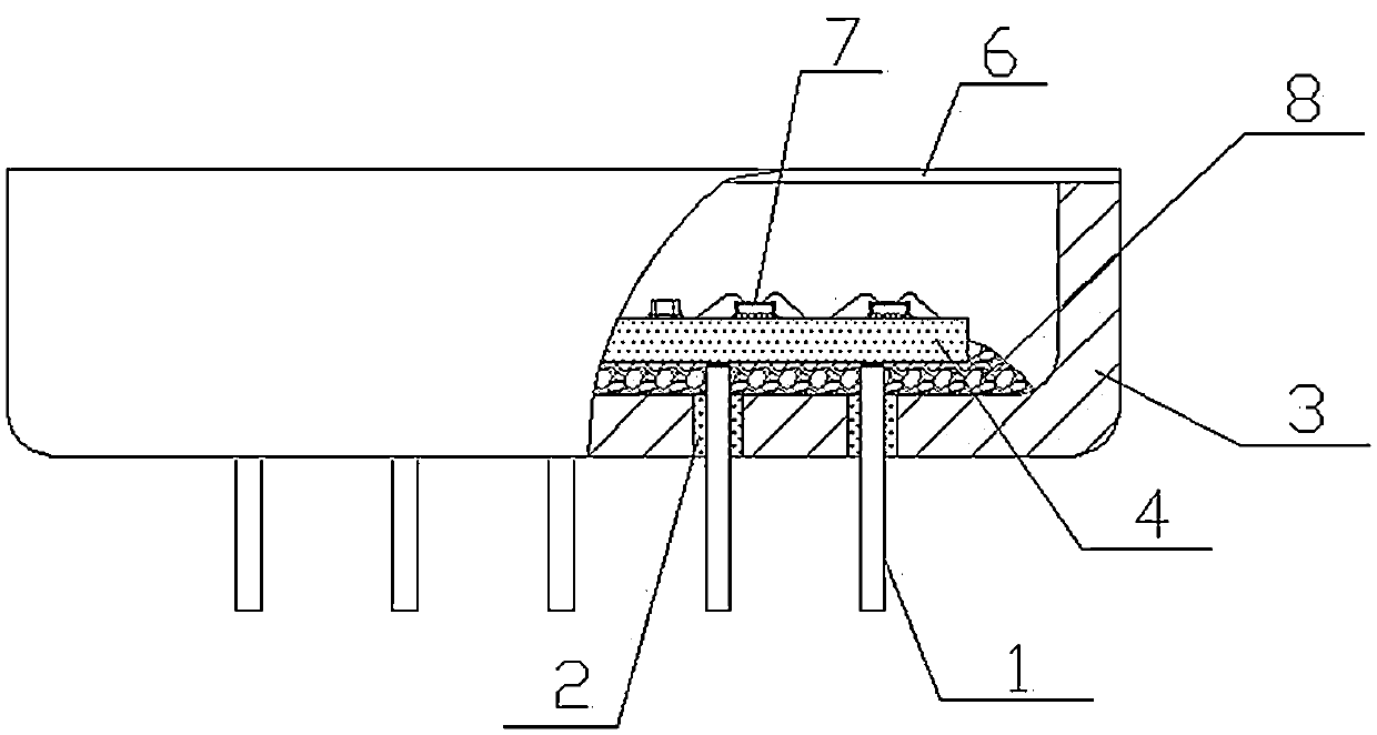
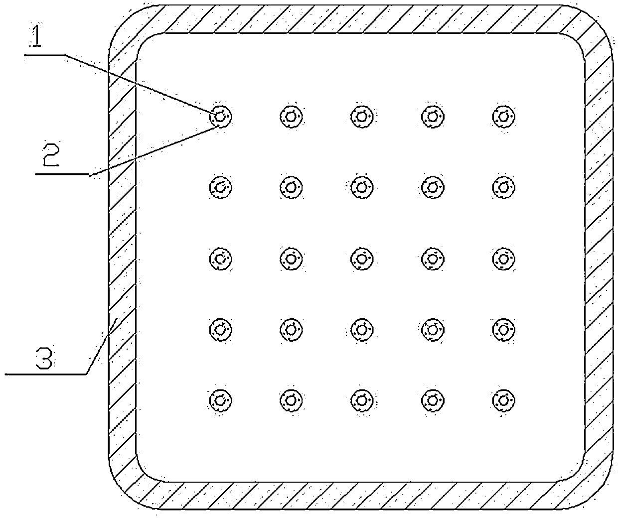
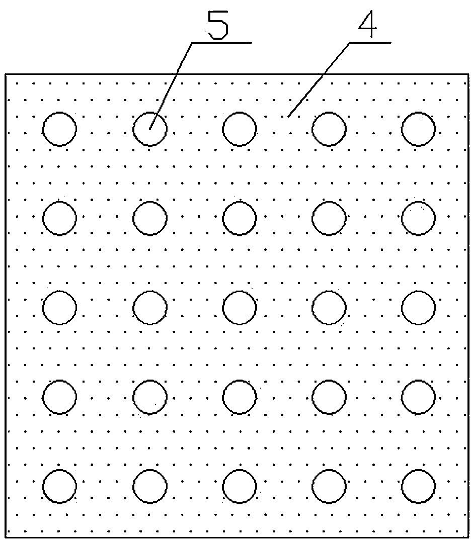
[0012] combine figure 1 and figure 2 As shown, the present invention provides a ceramic substrate assembly device, comprising a metal shell base 3 and a ceramic substrate 4 disposed in the metal shell base 3, the top surface of the ceramic substrate 4 is provided with components 7; the bottom surface of the metal shell base 3 There are arrayed outer pins 1 penetrating through the metal shell base 3, and the insulating medium 2 is used for sintering between the arrayed outer pins 1 and the metal shell base 3, and the insulating medium 2 can be a glass insulator; image 3 As shown, the bottom surface of the ceramic substrate 4 is provided with an array of pads 5 corresponding to the arrayed outer pins 1, the area of ​​the pads is greater than the area of ​​the ends of the outer pins, and the ceramic substrate 4 and the arrayed outer pins 1 are welded together. The disk array 5 is welded; the bottom surface of the ceramic substrate 4 and the metal shell base 3 are filled and bo...


PUM


Abstract

The invention discloses a ceramic substrate assembling device which comprises a metal outer shell base (3) and a ceramic substrate (4) arranged in the metal outer shell base (3). A component (7) is arranged on the top face of the ceramic substrate, array type outer pins (1) which penetrate through the metal outer shell base are arranged on the bottom face of the metal outer shell base, and the outer pins and the metal outer shell base are sintered by insulation media. Welding plate arrays (5) corresponding to the array type outer pins are arranged on the bottom face of the ceramic substrate, and the ceramic substrate and the outer pins are welded through the welding plate arrays. The bottom face of the ceramic substrate and the metal outer shell base are bonded through bonding glue in a filling mode. A metal cover plate is welded on the top of the metal outer shell base in a sealing mode. The ceramic substrate is not directly exposed, and good protection can be achieved. The outer pins and the metal outer shell base are sintered integrally, and the outer pins can not be disengaged from the surface of the substrate easily. The ceramic substrate is connected with the outer pins and the metal outer shell base respectively, a combination assembling structure is achieved, the assembling strength between the ceramic substrate and the metal outer shell base is improved, and the impact performance is improved.

Description

technical field [0001] The invention relates to the field of electronic manufacturing, in particular to a ceramic substrate assembly device. Background technique [0002] As we all know, ceramic substrates are increasingly used in electronic circuits due to their excellent electrical insulation properties and high thermal conductivity; at present, there are usually three structures for the assembly device of ceramic substrate products: 1. The bottom surface of the substrate is welded to the outside of the product. Feet, the metal frame is welded around the top surface of the substrate, and the top surface of the substrate is sealed and welded by the metal cover plate and the metal frame to realize the package. Due to the brittle characteristics of ceramic materials, the substrate under this structure is vulnerable to damage under the action of external mechanical impact stress , the outer pins are directly welded to the surface of the ceramic substrate, and the bonding stren...

Claims


Application Information

Patent Timeline
IPC IPC(8): H05K3/30H05K13/04
Inventor 夏俊生李寿胜侯育增李文才
Owner EAST CHINA INST OF OPTOELECTRONICS INTEGRATEDDEVICE
Why Eureka
Try Eureka