Array substrate, driving method and display device

An array substrate and substrate technology, which is applied in static indicators, matching and classification, character and pattern recognition, etc., can solve the problems of increasing the thickness of the display screen, and achieve the effect of reducing the difficulty of manufacturing and reducing the thickness.

Inactive Publication Date: 2014-12-10
BOE TECH GRP CO LTD +1
View PDF6 Cites 27 Cited by
  • Summary
  • Abstract
  • Description
  • Claims
  • Application Information

AI Technical Summary

Problems solved by technology

However, on the one hand, such a design will increase the thickness of the display screen, and on the other han

Method used


Image

  • Array substrate, driving method and display device
  • Array substrate, driving method and display device
  • Array substrate, driving method and display device

Examples


Embodiment Construction

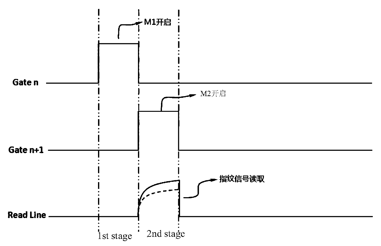
[0026] The specific implementation manners of the present invention will be further described in detail below in conjunction with the accompanying drawings and embodiments. The following examples are used to illustrate the present invention, but are not intended to limit the scope of the present invention.

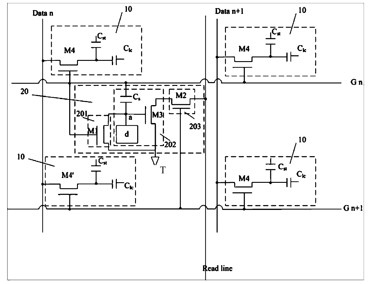
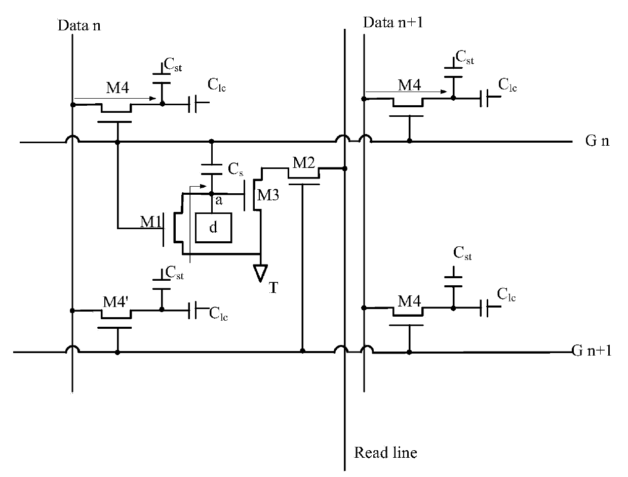
[0027] An embodiment of the present invention provides an array substrate, the array substrate includes a base,

[0028] The substrate is formed with: a plurality of fingerprint identification circuits for fingerprint identification, fingerprint signal reading lines, initialization signal lines, common voltage input terminals, and output control signal lines; each fingerprint identification circuit includes an initialization unit, a fingerprint identification unit and the output control unit, where,

[0029] The initialization unit is connected to the fingerprint identification unit, and is connected to the common voltage input terminal and the corresponding initializatio...


PUM


Abstract

The invention discloses an array substrate, a driving method and a display device for a fingerprint identification circuit. The array substrate comprises a substrate, wherein the fingerprint identification circuit, a fingerprint signal reading wire, an initialized signal wire, a common voltage input end and an output control signal wire are formed on the substrate. Therefore, on one hand, due to the fact that an independent film layer or face plate does not need to bear the fingerprint identification circuit, the thickness of the corresponding display device can be reduced; on the other hand, the fingerprint identification circuit and related signal wires can be formed at the same time while the array substrate is manufactured, so that the manufacturing difficulty for the corresponding display device is reduced.

Description

technical field [0001] The invention belongs to the field of display technology, and in particular relates to an array substrate, a driving method and a display device. Background technique [0002] With the increasing maturity of fingerprint identification technology, its application is becoming more and more extensive. In the display screens of some consumer electronic products (such as mobile phones, PDAs, etc.), fingerprint identification functions have also begun to be introduced. In the prior art, generally, a panel or a film layer containing a fingerprint identification circuit is directly pasted on the display panel to form a display screen with a fingerprint identification function. However, on the one hand, such a design will increase the thickness of the display screen, and on the other hand, it also requires a separate process to manufacture the corresponding fingerprint recognition panel or film layer. Contents of the invention [0003] The purpose of the pr...

Claims


Application Information

Patent Timeline
IPC IPC(8): G09G3/20G06K9/00
CPCG06V40/1365G06V40/1306
Inventor 杨盛际董学王海生郭仁炜许静波
Owner BOE TECH GRP CO LTD
Why Eureka
Try Eureka