
Flash memory burner, burning system and burning method

A flash memory and flash memory storage technology, applied in the electronic field, can solve the problems of unable to monitor the operation process, slow copy speed, poor scalability, etc., and achieve the effect of simplifying the programming control process, improving mass production efficiency, and speeding up the programming speed

Active Publication Date: 2014-12-10
WUXI ZGMICRO ELECTRONICS CO LTD
View PDF5 Cites 16 Cited by
  • Summary
  • Abstract
  • Description
  • Claims
  • Application Information

AI Technical Summary

Problems solved by technology

[0006] 1) The copying speed is slow, and the time-consuming increases with the increase of the number of pieces burned;
[0007] 2) The operation steps are complicated, and the operation procedures on the market basically require more than 4 steps;
[0008] 3) The burn-in device has high cost and poor scalability;
[0009] 4) The burner operates semi-automatically, and cannot automatically check for bad chips, blank checks, programming, erasing, etc.;
[0010] 5) The operation process cannot be monitored, and effective prompts cannot be given;
[0011] 6) It is impossible to count the number of burned-in films (such as bad films and good films);
[0012] 7) Unable to write the specified Bluetooth Address (Bluetooth address) and Device Name (device name) to each chip;

Method used


Image

  • Flash memory burner, burning system and burning method
  • Flash memory burner, burning system and burning method
  • Flash memory burner, burning system and burning method

Examples


Embodiment Construction

[0045] The specific embodiments of the present invention will be described below in conjunction with the drawings in the specification.

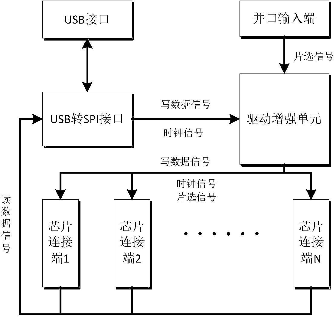
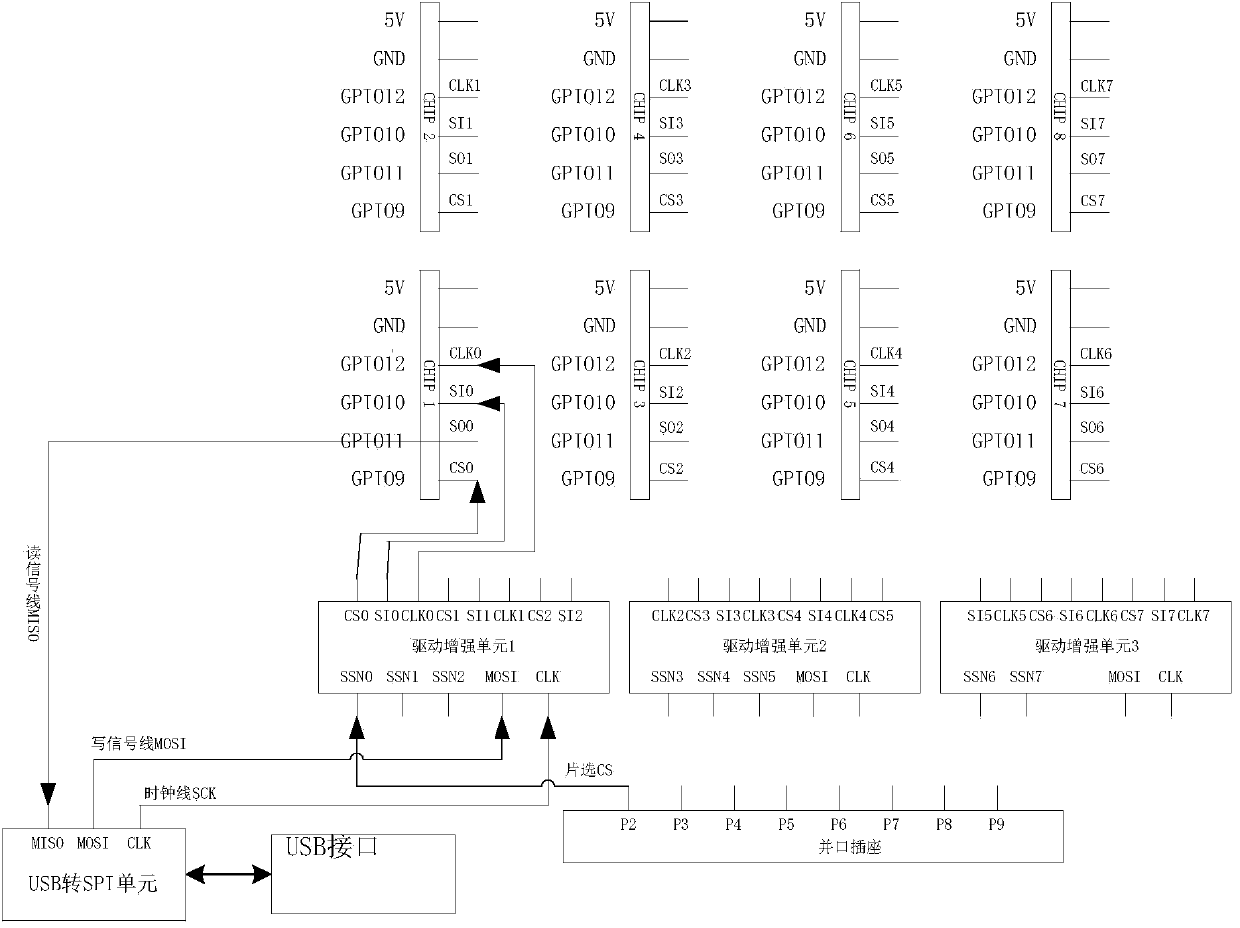
[0046] reference figure 1 As a specific implementation of the present invention, a flash memory burner can simultaneously burn the flash memory of multiple Bluetooth chips, including parallel port input, USB interface, USB to SPI unit and multiple chip connection terminals;

[0047] The parallel port input terminal is used to output a plurality of chip selection signals corresponding to each chip connection terminal;

[0048] The USB interface provides a transmission channel for a read data signal and a write data signal;

[0049] The USB to SPI unit is used for reading and writing data processing, and realizes the communication between the USB bus and the SPI interface. When the chip select signal is valid, it outputs the write data signal from the USB interface to each chip connection terminal, and Outputting the read data signal from the chip con...


PUM


Abstract

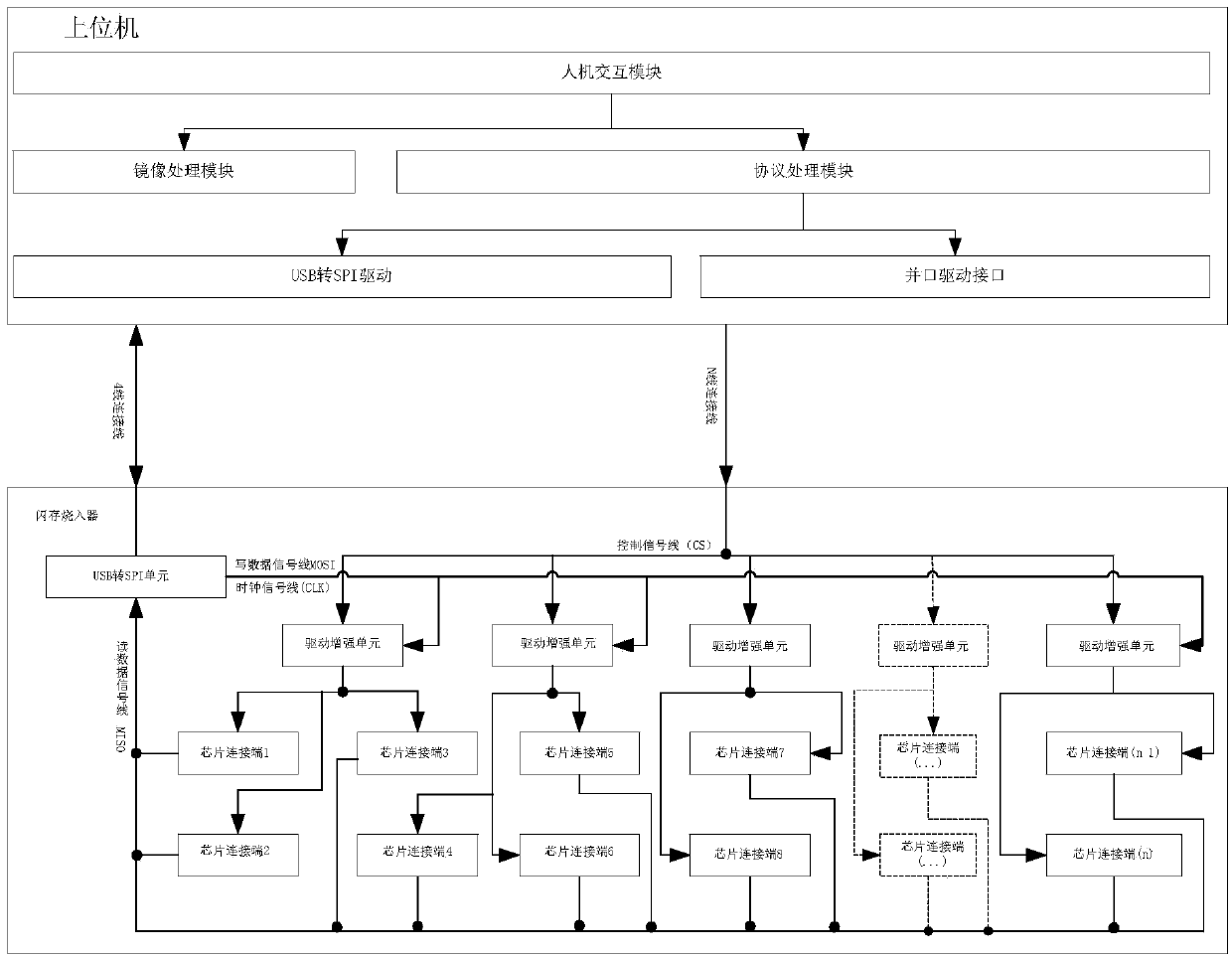
The invention discloses a flash memory burner, a burning system and a burning method. Flash memories of a plurality of bluetooth chips can be simultaneously burnt, the number of the simultaneously burnt chips can be changed through the parallel transmission of chip select signals, the different requirements of one-step burning and one-to-one burning can be met, the operation is more flexible, and the application range is wider. Besides, as the memory positions of bluetooth addresses and equipment names are previously stored in an image file, the memory position information can be acquired when the image file is burnt, and corresponding to-be-burnt addresses in to-be-burnt chips can be found according to the memory position information. Therefore, the bluetooth addresses and the equipment names can be directly burnt after the image file is burnt, burning is no longer needed to be carried out after erasing like the prior art, the burning process of the flash memories of the bluetooth chips is essentially changed, the burning speed is raised, and the burning control procedures are simplified and more tend to automation.

Description

Technical field [0001] The invention relates to the field of electronics, in particular to a high-efficiency flash memory burner, a burning system and a burning method. technical background [0002] Burner is a tool for writing data on programmable integrated circuits. It is mainly used for programming (or flashing) of chips such as single-chip microcomputer (including embedded) / memory (including BIOS). It can be divided into functions. Universal burner, mass production burner, special burner. [0003] The existing mass-produced burners are usually connected to a burner through a computer, a software runs in the computer to control burning and opening the program files to be burned, and then transfer data to the burner via USB or serial port to burn The receiver then transmits it to the chip. [0004] However, some of the existing mass-produced Bluetooth flash memory (flash) burners cannot burn multiple chips at a time, and their work efficiency is extremely low; some only support ...

Claims


Application Information

Patent Timeline
Patent Type & Authority Applications(China)
IPC IPC(8): G11C16/10
Inventor 邹世彬
Owner WUXI ZGMICRO ELECTRONICS CO LTD
Learn More