Sunken type soft and hard combined circuit board and manufacturing method thereof

A soft-rigid combination and manufacturing method technology, applied in the direction of multilayer circuit manufacturing, printed circuit components, printed circuit structural connection, etc., can solve the problem that the thickness of the camera chip cannot be reduced, and can no longer be reduced

Inactive Publication Date: 2014-12-17
深圳市华大电路科技有限公司
View PDF3 Cites 12 Cited by
  • Summary
  • Abstract
  • Description
  • Claims
  • Application Information

AI Technical Summary

Problems solved by technology

Tracing it to its cause is that existing high-pixel camera circuit boards are all made of R-F circuit boards (mostly four-layer boards), such as figure 1 As shown, it consists of the middle soft board 4, the hard board 5 pasted on the soft board, and the hard board 6 pasted under the soft board. The combined board is also above 0.25mm, and then the camera chip is added to the thick hard board. The thickness of the camera chip itself cannot be reduced. Finally, the thickness of the lens holder is added to the camera chip. The entire thickness can no longer be reduced. As a result, the overall thickness of the camera is thicker than the fuselage and protrudes

Method used


Image

  • Sunken type soft and hard combined circuit board and manufacturing method thereof
  • Sunken type soft and hard combined circuit board and manufacturing method thereof
  • Sunken type soft and hard combined circuit board and manufacturing method thereof

Examples


Embodiment 1

[0049] Step 1: Make the inner soft board of the soft-hard board

[0050] (1) Cutting

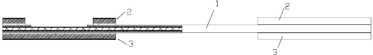
[0051] The Dsflex600122512R P double-sided adhesive-free calendered copper coil material from Doosan, South Korea is used as the raw material of the flexible board, and the copper clad laminate consists of three layers: copper foil layer 12 on the soft board, PI layer 13 on the soft board, and copper foil layer under the soft board. 14. Use a cutting machine to cut it into sheets with a size of 250*190mm. The thickness of the copper foil layer 12 on the flexible board and the copper foil layer 14 under the flexible board are both 12um, and the PI layer 13 of the flexible board in the middle is 25um.

[0052] (2) Dry film, exposure, development, etching and film withdrawal; detection

[0053] On the upper surface of the copper foil layer 12 on the soft board of the described copper clad board and the lower surface of the lower copper foil layer 14 of the soft board, dry films are pasted wit...


PUM


Abstract

The invention provides a sunken type soft and hard combined circuit board. The sunken type soft and hard combined circuit board comprises an inner layer soft plate, an upper hard plate and a lower hard plate, wherein a line graph is distributed on the inner layer soft plate; the upper hard plate and the lower hard plate are respectively pressed to and combined with the upper and lower surfaces of the inner layer soft plate; a concave groove in which a sensor can be mounted is formed and downwards passes through the sensor on the upper surface of the upper hard plate to reach the inner part of the inner layer soft plate, and therefore, the finished product is five layer less than the traditional soft and hard combined circuit board, and as a result, a chip can be embedded for at least 0.12mm, and the thickness of the whole electronic product can be reduced by more than 0.12mm. The invention also provides a preparation method of the sunken type soft and hard combined circuit board. The method comprises the following steps: forming a window in the upper hard plate and forming a window with a covering film of the inner layer soft plate; forming a loop of bosses around a copper coil on the exposed soft plate through the formed windows; cutting with laser and gasifying to remove the loop of bosses to form the concave groove with tidy side angles. With the adoption of the manufacturing method, the gummosis phenomenon is avoided, thus the concave groove can be in a complete state, and the bottom surface of the concave groove is flat and out of bulking, and as a result, the imaging effect of a camera can be ensured.

Description

technical field [0001] The invention relates to a method for manufacturing a printed circuit board, in particular to a sinking type soft-hard combination circuit board and a method for manufacturing the same. Background technique [0002] At present, the hardware performance of smartphones has undergone earth-shaking changes. From single-core to dual-core to quad-core, many mobile phone manufacturers are also fighting for success in the arms race. However, at the same time, as far as the current situation is concerned, the performance of quad-core mobile phones has already been excessive for most users. Compared with the current system and software application level, excessive hardware configuration often means more waste of resources, consumption Readers gradually began to bid farewell to the irrational behavior of purely pursuing hardware performance. In this context, the research and development focus of smartphones will definitely change, and ultra-thin has become the n...

Claims


Application Information

Patent Timeline
Patent Type & Authority Applications(China)
IPC IPC(8): H05K1/14H05K3/36H05K3/46
Inventor 陈维恩文桥孙建光郭瑞明
Owner 深圳市华大电路科技有限公司
Why Eureka
Try Eureka