Leakage defect detection method

A defect, positive charge technology, applied in the field of semiconductor reliability analysis, which can solve problems such as noise interference, inability to quantify the severity in detail, and blurred image brightness.

Inactive Publication Date: 2014-12-24
SEMICON MFG INT (SHANGHAI) CORP
View PDF9 Cites 6 Cited by
  • Summary
  • Abstract
  • Description
  • Claims
  • Application Information

AI Technical Summary

Problems solved by technology

The voltage contrast detection of a single negative charge mode requires a higher LE in order to obtain a stable image brightness
Experiments have proved that although the voltage contrast detection in the negative charge mode can accurately detect high-risk leakage defects, the long-term high voltage and high current will cause a large amount of interference charges to accumulate on the sample surface of the semiconductor device, which will eventually cause a large blur in the image brightness. noise disturbance
[0004] The problem with the voltage contrast detection using the positive charge mode is that because the leakage defect itself has different mechanis...

Method used


Image

  • Leakage defect detection method
  • Leakage defect detection method

Examples


Embodiment Construction

[0022] In order to make the object, technical solution, and advantages of the present invention clearer, the present invention will be further described in detail below with reference to the accompanying drawings and examples.

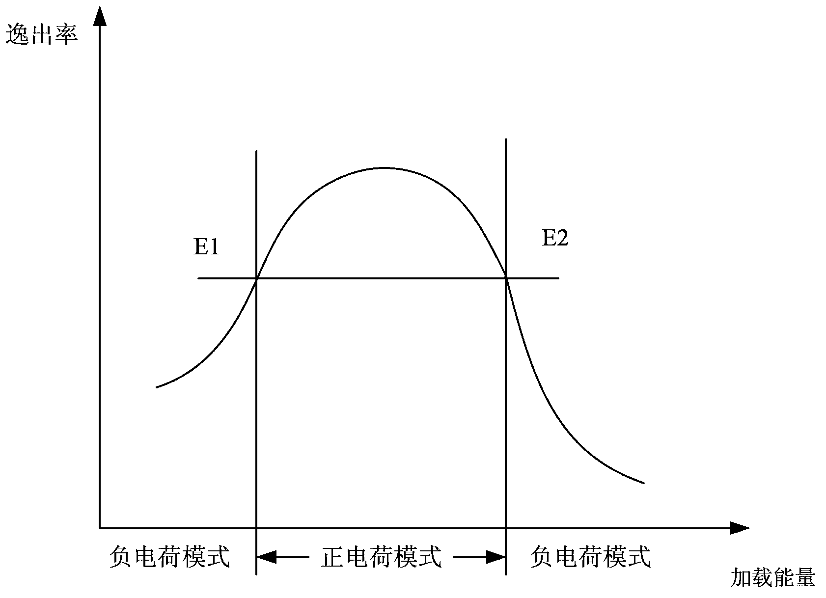
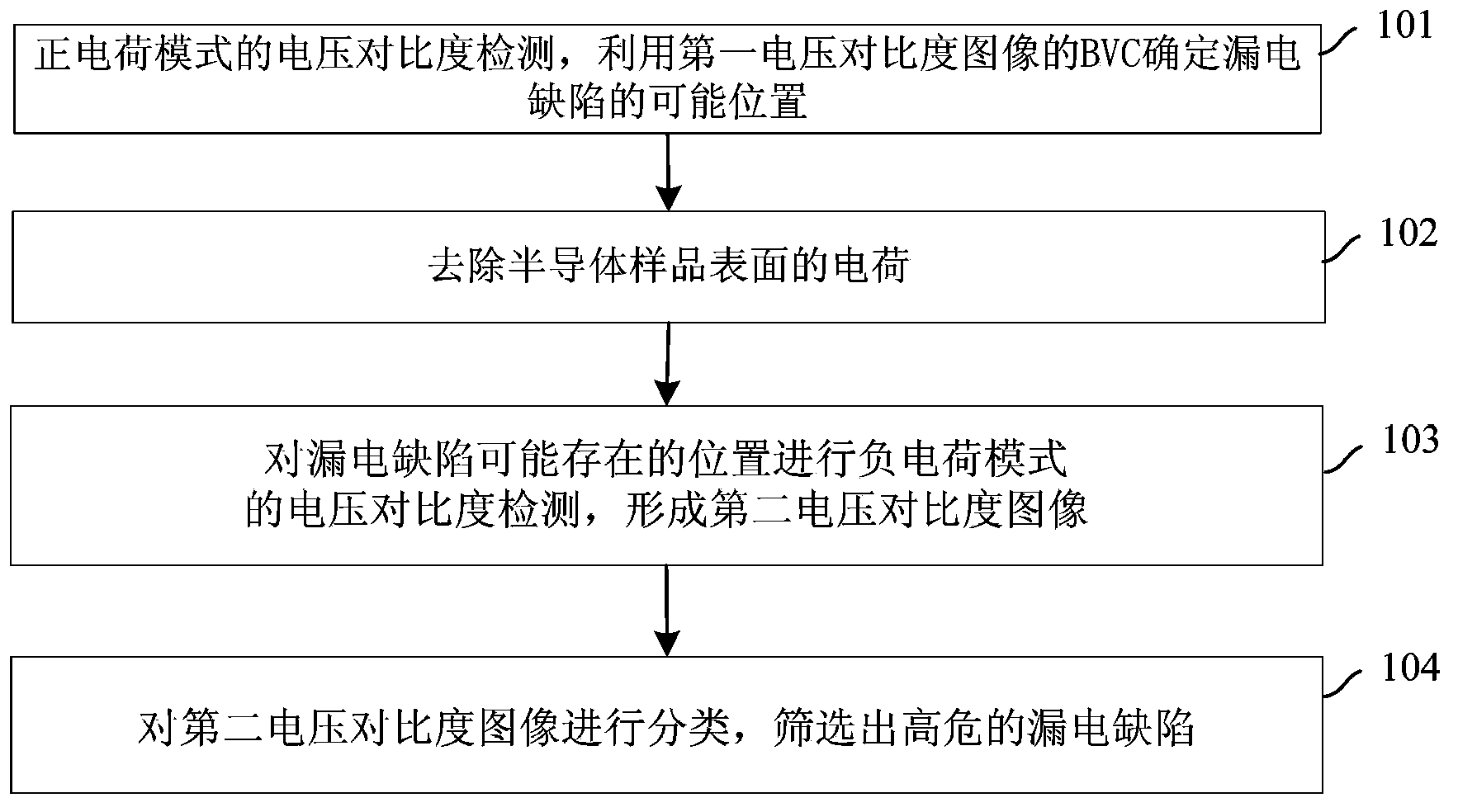
[0023] The present invention proposes a leakage defect detection method, the specific steps are as follows figure 2 As shown, this method can accurately detect high-risk leakage defects in semiconductor samples. In this specific embodiment, the semiconductor sample as the detection object of voltage contrast detection is specifically CT WCMP layer, and the high-risk defects in CT WCMP layer are screened out through voltage contrast detection. Leakage defects.

[0024] Step 101 , positive charge mode voltage contrast detection of semiconductor samples, forming a first voltage contrast image, using the bright defect (BVC) in the first voltage contrast image to determine the possible location of the leakage defect.

[0025] In this step, the method and ...


PUM


Abstract

The invention provides a leakage defect detection method. According to the method, a first voltage contrast image with high-definition BVC is obtained by means of voltage contrast detection in a positive mode, a potential leakage defect position in a semiconductor sample is captured, then a second voltage contrast image is obtained by scanning the position of the BVC again by means of voltage contrast detection in a negative mode, the BVC is screened by means of the DVC of the second voltage contrast image so that accurate BVC classification can be achieved, and a high-purity high-risk leakage defect is obtained.

Description

technical field [0001] The invention relates to a semiconductor reliability analysis method, in particular to a leakage defect detection method. Background technique [0002] At present, there are various reliability analysis methods for semiconductor devices, among which the voltage contrast (Voltage Contrast, VC) detection method has been widely used. The voltage contrast detection method usually uses a scanning electron microscope (Scanning Electron Microscopy, SEM) to perform voltage contrast detection on samples of semiconductor devices. The principle is to excite secondary electrons by bombarding the surface of the sample with a focused electron beam (E-beam). The material properties of the sample determine the number of secondary electrons generated, so the material of the bombarded sample is different, and the number of secondary electrons collected is also different, and the number of secondary electrons is expressed as image brightness , so as to determine whether...

Claims


Application Information

Patent Timeline
IPC IPC(8): G01R31/02
Inventor 赵宁吴浩田唯磊戴腾任保军
Owner SEMICON MFG INT (SHANGHAI) CORP
Why Eureka
Try Eureka