Efficient cadmium telluride nanocrystalline Schottky junction solar cell with modified anode interface and preparing method thereof

An anode interface, solar cell technology, applied in circuits, photovoltaic power generation, electrical components, etc., can solve problems such as unfavorable carrier separation and extraction, affecting hole transport, etc., to improve the solar open circuit voltage and fill factor, achieve ohmic Contact, the effect of enhancing stability

Inactive Publication Date: 2014-12-24
SOUTH CHINA UNIV OF TECH
View PDF3 Cites 7 Cited by
  • Summary
  • Abstract
  • Description
  • Claims
  • Application Information

AI Technical Summary

Problems solved by technology

[0004] However, the current cadmium telluride nanocrystalline solar cells have certain problems: light is incident from the anode side of ITO, and the photogenerated electrons need to go through a relatively thick active layer to reach the cathode, and are easily recombined during the transmission process, which is not conducive to Separation and extraction of carriers; on the other hand, according to Schottky theory, to make P-type CdTe form an ohmic contact with the anode, the work function of the anode must be higher than that of CdTe
However, the work function of ITO is lower than that of CdTe, and it will inevitably form a Schottky diode opposite to CdTe / Al, which will affect the hole transport.

Method used


Image

  • Efficient cadmium telluride nanocrystalline Schottky junction solar cell with modified anode interface and preparing method thereof
  • Efficient cadmium telluride nanocrystalline Schottky junction solar cell with modified anode interface and preparing method thereof
  • Efficient cadmium telluride nanocrystalline Schottky junction solar cell with modified anode interface and preparing method thereof

Examples


preparation example Construction

[0035] 2. Preparation of anode interface layer material:

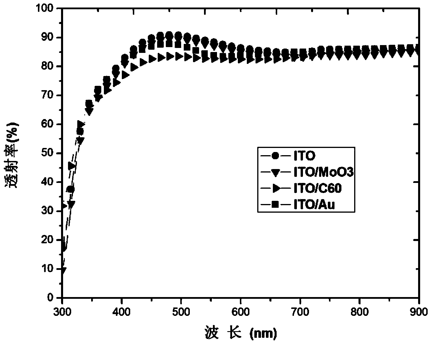
[0036] When choosing Au or MoO X (x value is 2~3) When it is used as the anode interface layer material, put the cleaned and dried ITO substrate into the DM-300B vacuum coating chamber for plating, turn on the mechanical pump and molecular pump, and when the coating chamber reaches 3 ×10 -4 Start to evaporate Au or MoO after the high vacuum of Pa X , the evaporation rate and thickness are monitored in real time by a quartz vibrator film thickness monitor, and the evaporation rate is When choosing C 60 When used as an anode interface layer material, C 60 The anode interface layer was prepared by solution processing, and the C 60 Dissolved in p-xylene to obtain a purple solution with a concentration of 5mg / ml, the solution was spin-coated on the ITO substrate at different speeds to obtain different thicknesses of C 60 The film was heated at 200°C for 20 minutes, and finally a uniform and light-transmitting C 60 f...

Embodiment 1

[0044] Embodiment 1 Different thickness MoO X Effect on Device Performance

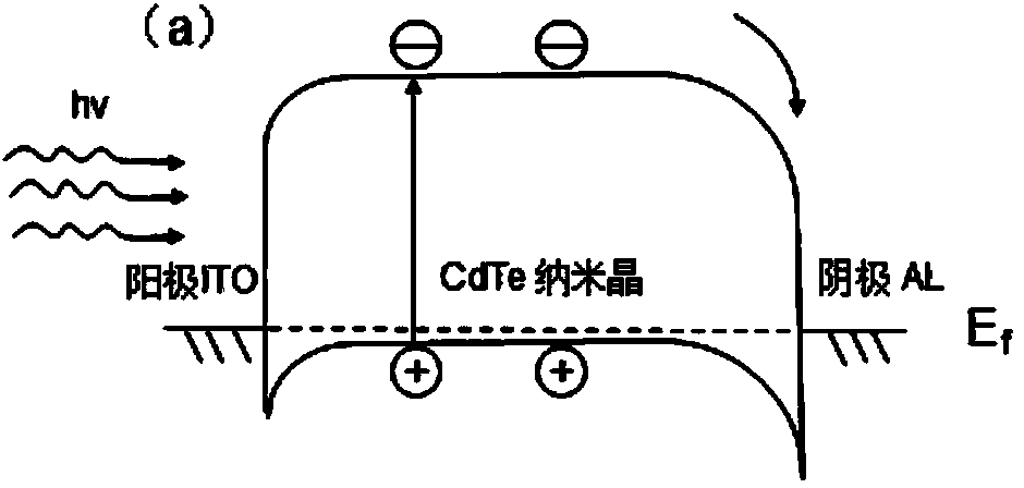
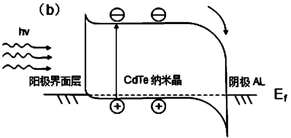
[0045] According to the Schottky theory, to make the P-type cadmium telluride form a stable ohmic contact with the anode, the work function of the anode must be higher than that of the active layer cadmium telluride. Then the work function of the anode ITO is only 4.7, while the work function of the active layer CdTe is about 5.1 to 5.3. When the two materials are in contact, electrons will flow from one side of the low work function (ITO) to the other side (CdTe) until Fermi The energy level is equal. Thus, the anode ITO will be slightly positively charged while the high work function material CdTe will become slightly electronegative. Finally, a built-in electric field is formed at the interface, causing the energy band at the semiconductor interface to bend downward, which affects the extraction and collection of holes, such as Figure 1a shown. On the contrary, adding a layer of high work funct...

Embodiment 2

[0050] Embodiment 2 Effect of different thicknesses of Au on device performance

[0051] Repeat Example 1, select high work function metal Au (work function is 5.1eV) as the anode interface layer, the thickness is respectively 0.5nm, 1nm, 2nm, other conditions remain unchanged. The experimental results are summarized in Table 3.

[0052]It can be seen from Table 3 that the addition of Au significantly improves the open circuit voltage and fill factor, especially the device optimization effect of 1nm Au is the best, the open circuit voltage and fill factor are increased by 22% and 39% respectively, and the overall efficiency is increased from 4.3% to 5.3%. Since Au has a large absorption in the visible light range, as the thickness of Au increases, the light absorption of the active layer will decrease, and the current will continue to decrease. Compared with 0.5nm Au, the addition of 1nm Au can form a more uniform and dense island-like Au, fully realize the ohmic matching be...


PUM

PropertyMeasurementUnit
thicknessaaaaaaaaaa
thicknessaaaaaaaaaa
thicknessaaaaaaaaaa

Abstract

The invention discloses an efficient cadmium telluride nanocrystalline Schottky junction solar cell with a modified anode interface and a preparing method of the solar cell. The solar cell is formed by stacking a glass substrate, an anode, an anode interface layer, an optical activity layer and a cathode in sequence. The anode interface layer is added between the anode and the active layer so that anode work function control can be performed, and the anode interface layer is made from Au or MoOX or C60. Anode interface material has high work function. The anode interface material is deposited on an anode substrate in a vacuum evaporation mode or dissolved in organic solvent to prepare solution, and finally, the anode interface layer is formed on the anode substrate. The energy conversion efficiency of the cadmium telluride nanocrystalline Schottky junction solar cell can be obviously improved, the curling phenomenon of an I-V curve is avoided to some extent, the characteristic of a diode is enhanced, and the service life of devices is prolonged. According to the efficient cadmium telluride nanocrystalline Schottky junction solar cell with the modified anode interface and the preparing method of the solar cell, the preparing technology is simple, the main preparing process can be completed in a common fume hood through solution, and the manufacturing cost is greatly reduced.

Description

technical field [0001] The invention relates to the field of photoelectric devices, in particular to an anode interface modified high-efficiency cadmium telluride nanocrystal Schottky junction solar cell and a preparation method thereof. Background technique [0002] With the development of science and technology and material civilization, human needs for energy are increasing. As the mineral energy and atomic energy that humans rely on most at present, its disadvantages are becoming more and more obvious. So people turn their attention to clean and renewable energy such as solar energy, but to compete with traditional energy sources, solar cells must first achieve new breakthroughs in the following two aspects: one is to reduce the production cost of existing solar cells, mainly Reduce the cost of raw materials and energy consumption; the second is to improve the photoelectric conversion efficiency of solar cells, that is, to improve the performance-price ratio of batterie...

Claims


Application Information

Patent Timeline
Patent Type & Authority Applications(China)
IPC IPC(8): H01L31/0296H01L31/18
CPCH01L31/022425H01L31/03925H01L31/1828Y02E10/543Y02P70/50
Inventor 覃东欢朱娇燕高玉萍杨跃骅
Owner SOUTH CHINA UNIV OF TECH
Why Eureka
Try Eureka