Scanning signal line drive circuit and display device provided with same

A technology for scanning signal lines and driving circuits, which is applied in the field of active matrix display devices, can solve problems such as increased load and increased power consumption, and achieve the effects of reducing power consumption and suppressing electromagnetic interference (EMI)

Inactive Publication Date: 2014-12-24
SHARP KK
View PDF10 Cites 16 Cited by
  • Summary
  • Abstract
  • Description
  • Claims
  • Application Information

AI Technical Summary

Problems solved by technology

This scanning signal line driving circuit includes a shift register circuit, but due to the enlargement and high definition of the display device, the load connected to the output of each stage of the shift register circuit increases, and the power consumption also increases.

Method used


Image

  • Scanning signal line drive circuit and display device provided with same
  • Scanning signal line drive circuit and display device provided with same
  • Scanning signal line drive circuit and display device provided with same

Examples


no. 1 Embodiment approach >

[0062]

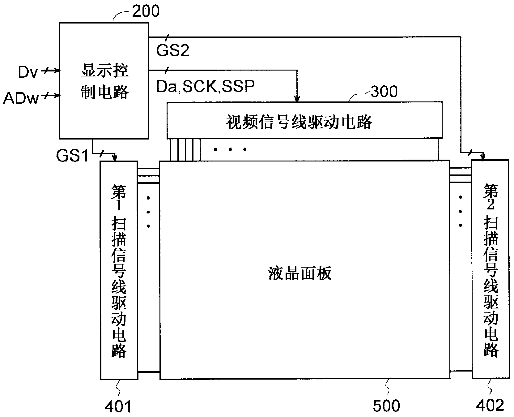
[0063] figure 1 It is a block diagram showing the configuration of a liquid crystal display device according to an embodiment of the present invention. The liquid crystal display device comprises: a display control circuit 200; a video signal line drive circuit (also referred to as a "source drive circuit" or a "column electrode drive circuit") 300; a first and a second scanning signal line drive circuit (the circuit Also referred to as “gate drive circuit”, “row electrode drive circuit”) 401 , 402 ; and active matrix type liquid crystal panel 500 .

[0064] Among these circuits, the above-mentioned first and second scanning signal line driver circuits 401 and 402 are integrally formed (so-called monolithic) on an element substrate which is a glass substrate together with a pixel circuit described later, and the display control circuit 200 and the video signal The line driver circuit 300 is formed in an IC chip and mounted on an element substrate. A liquid crysta...

no. 2 Embodiment approach >

[0108]

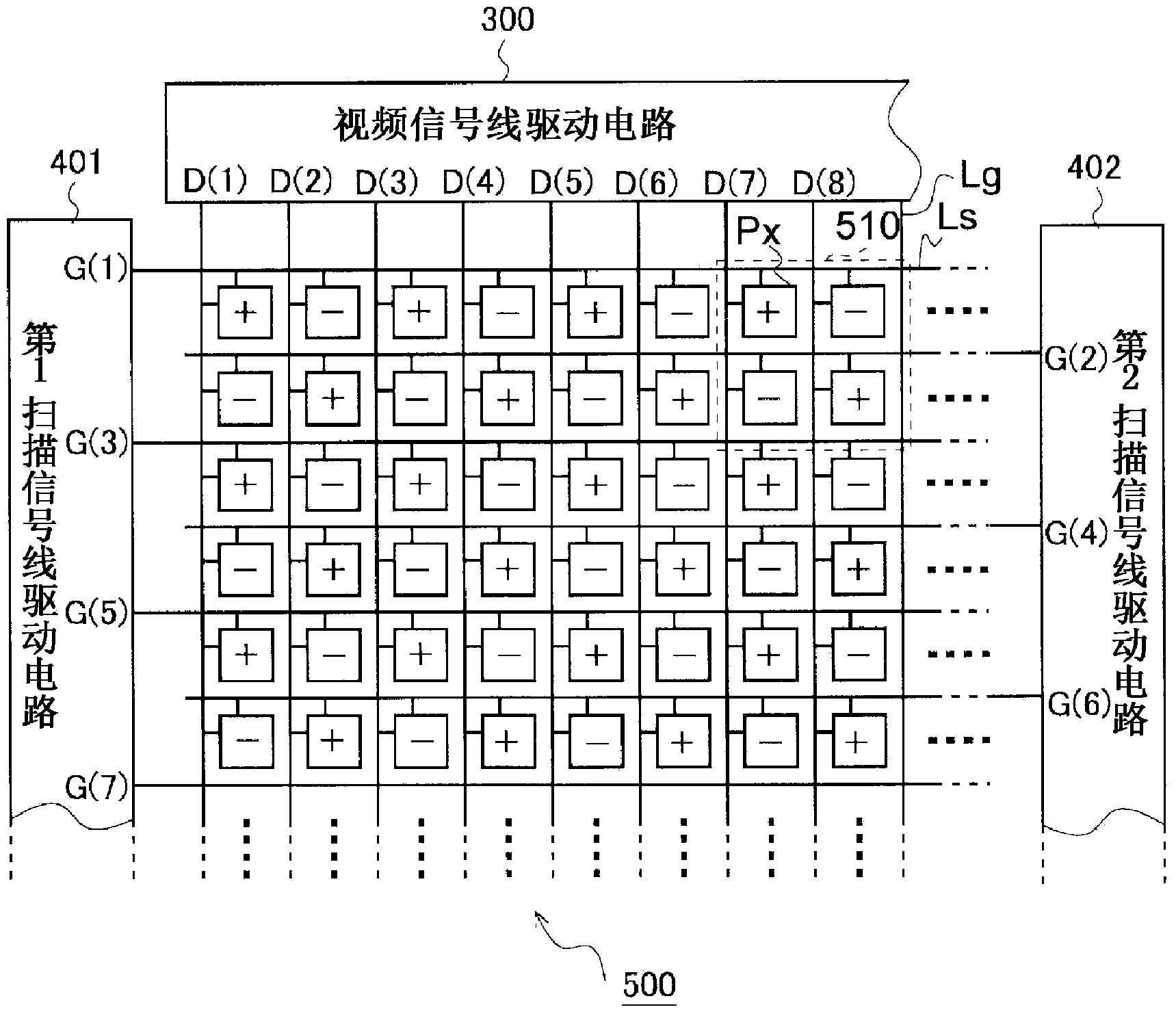
[0109] The configuration and the figure 1 The configuration shown is the same, and the configuration of the liquid crystal panel 500 is also the same as image 3 etc. are the same, and therefore, the same reference numerals are attached to the same constituent elements, and detailed descriptions are omitted. In addition, the configurations of the shift register circuits included in the first and second scanning signal line driving circuits 401 and 402 are also the same, but their operations are slightly different. In addition, related to this, the scanning signal lines connected to the first and second scanning signal line drive circuits 401 and 402 are different from those of the first embodiment. Below, refer to Figure 9 Explain in detail.

[0110] Figure 9 It is a diagram for explaining the selection and connection relationship of scanning signal lines and the relationship between each signal. with the above Figure 7 The composition shown is different, ...

no. 3 Embodiment approach >

[0119]

[0120] The configuration and the figure 1 The configuration shown is the same, and the configuration of the liquid crystal panel 500 is also the same as image 3 etc. are the same, and therefore the same components are given the same reference numerals and detailed descriptions are omitted. In addition, the configuration of the scanning signal line driver circuit is also the same as that of the first or second embodiment, and thus description thereof will be omitted.

[0121] In this embodiment, different from the first and second embodiments, the so-called time-division driving method is adopted, and the video signal lines Ls of the liquid crystal panel are divided into a plurality of video signal line groups in groups of three. The line group (three video signal lines Ls in the same group) is connected to one output terminal of the video signal line drive circuit 300 via the three analog switches in the same group. In this way, the output terminals of the video...


PUM


Abstract

First and second scanning signal line drive circuits (401, 402) provided to this liquid crystal display device perform interlaced driving. A gate clock signal, a gate start pulse signal, and a clear signal which are presented to these circuits are presented by sets of two trunk lines each, which correspond to the two shift register circuits respectively included therein. Consequently, the number of bistable circuits connected to a single trunk line is half that in a typical conventional scanning signal line drive circuit comprising a single shift register circuit, and moreover the clock signal frequency is lower, thereby further reducing power consumption.

Description

technical field [0001] The present invention relates to an active matrix type display device, and more particularly, to a scanning signal line driving circuit for an active matrix type display device. Background technique [0002] In general, liquid crystal display devices are driven by alternating current in order to suppress deterioration of liquid crystals. As this alternating driving method, there is known a driving method (frame inversion driving method) in which the polarity of the voltage applied to the liquid crystal is inverted every frame. However, according to this driving method, display defects such as flickering are likely to occur during display. Therefore, in recent years, not only inverting the positive and negative polarities of the applied voltage for each horizontal scanning line but also inverting the positive and negative polarities of the applied voltage for each frame has been adopted. The polarity inversion driving method (referred to as "line inver...

Claims


Application Information

Patent Timeline
Patent Type & Authority Applications(China)
IPC IPC(8): G09G3/36G02F1/133G09G3/20
CPCG09G3/2096G09G3/3614G09G3/3648G09G3/3688G09G2310/0227G09G2330/06G09G3/3677G09G2310/0213G09G2310/0224G09G2310/0286G09G2330/021
Inventor 横沼真介
Owner SHARP KK
Why Eureka
Try Eureka