

Method for manufacturing transparent conductive film, transparent conductive film, and electronic device
A technology of transparent conductive film and manufacturing method, which is applied in the direction of electric solid-state devices, semiconductor devices, organic semiconductor devices, etc., can solve the problems of high material cost, limited ITO resistance value, etc., and achieve excellent performance stability and sufficient conductivity Excellent light transmittance and water vapor barrier properties
- Summary
- Abstract
- Description
- Claims
- Application Information
AI Technical Summary
Problems solved by technology
Method used
Image

Examples
no. 1 Embodiment approach
[0032] 1. First Embodiment: First Configuration Example of Transparent Conductive Film
no. 2 Embodiment approach
[0033] 2. Second Embodiment: Second Configuration Example of Transparent Conductive Film
no. 3 Embodiment approach
[0034] 3. Third Embodiment: Configuration Example of Electronic Device
[0035] 4. Various embodiments
[0036]
[0037] [Overall configuration of transparent conductive film]
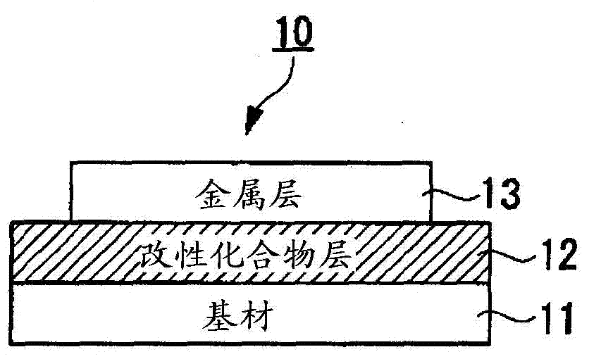
[0038] figure 1 A cross-sectional view of a schematic configuration of the transparent conductive film according to the first embodiment is shown in . In addition, "transparent" in this specification means that the light transmittance at a wavelength of 550 nm is 50% or more.
[0039] transparent conductive film 10, such as figure 1 As shown in , it includes: a substrate 11 , a modified compound layer 12 and a metal layer 13 . Furthermore, in the present embodiment, the modifying compound layer 12 and the metal layer 13 are sequentially laminated on one surface of the substrate 11 . be explained, figure 1 It is not shown in , but an anti-bleeding layer may be provided on the surface of the substrate 11 on the side of the modifying compound layer 12 . The anti-bleeding layer refers to a layer f...
PUM
| Property | Measurement | Unit |
|---|---|---|
| thickness | aaaaa | aaaaa |
| thickness | aaaaa | aaaaa |
| thickness | aaaaa | aaaaa |
Abstract
Description
Claims
Application Information