
Circuit board with embedded electronic component and manufacturing method of circuit board

A technology for electronic components and manufacturing methods, which is applied in the directions of printed circuits connected with non-printed electrical components, assembling printed circuits with electrical components, and electrically connecting printed components, etc. The positioning accuracy cannot be guaranteed, and the difficulty of forming blind holes and the precise alignment of solder terminals is increased.

Active Publication Date: 2014-12-31
AVARY HLDG (SHENZHEN) CO LTD +1
View PDF14 Cites 3 Cited by
  • Summary
  • Abstract
  • Description
  • Claims
  • Application Information

AI Technical Summary

Problems solved by technology

[0003] Using the above method to manufacture, there are the following problems: First, in the process of forming blind holes by laser, the alignment accuracy of the formed blind holes and soldering terminals cannot be guaranteed
Secondly, before the build-up, the soldering terminals of the electronic components are not soldered. During the build-up and lamination, the electronic components are prone to irregular deviation, which increases the precision between the subsequent blind holes and the soldering terminals. Difficulty of alignment

Method used


Image

  • Circuit board with embedded electronic component and manufacturing method of circuit board
  • Circuit board with embedded electronic component and manufacturing method of circuit board
  • Circuit board with embedded electronic component and manufacturing method of circuit board

Examples


Embodiment Construction

[0017] The circuit board manufacturing method provided by the technical solution includes the following steps:

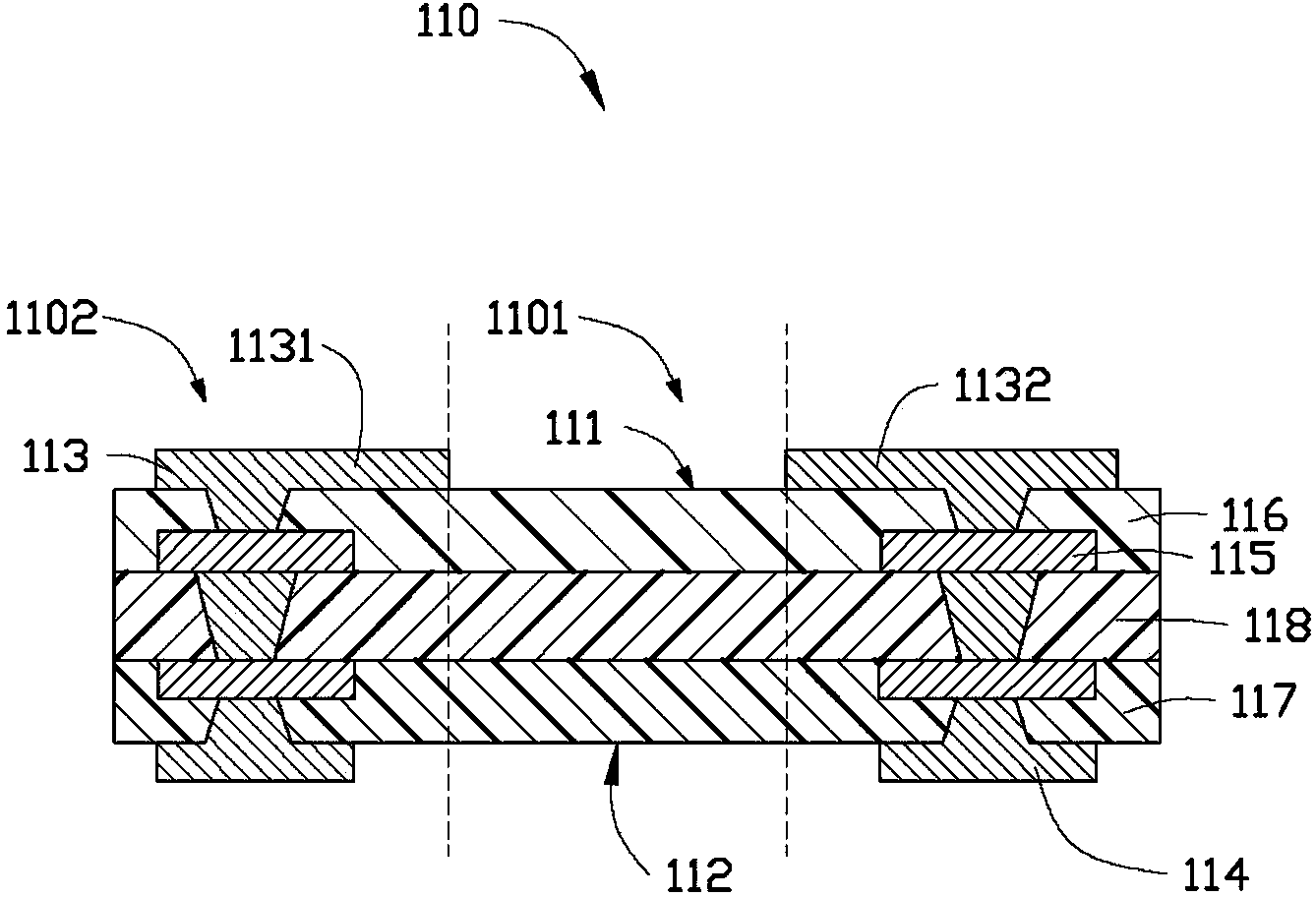
[0018] For a first step, see figure 1 , to fabricate the inner layer circuit substrate 110 .

[0019] The inner layer circuit substrate 110 is a circuit board formed with conductive lines. In this embodiment, the inner circuit substrate 110 is a four-layer circuit board, which includes four conductive circuit layers and three dielectric layers. Each dielectric layer is arranged between two adjacent conductive circuit layers. Conductive holes are formed in each dielectric layer, and two adjacent conductive circuit layers are electrically connected to each other through the conductive holes.

[0020] In this embodiment, the inner circuit substrate 110 has a first surface 111 and a second surface 112 opposite to each other. The first inner circuit layer 113 is formed on one side of the first surface 111 . The second inner circuit layer 114 is formed on one side of...


PUM


Abstract

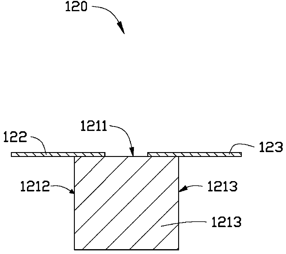
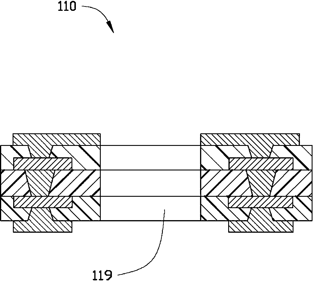
A circuit board with an embedded electronic component comprises an internal circuit substrate, the electronic component, a first layer-adding substrate and a second layer-adding substrate. The internal circuit substrate is provided with a first surface and a second surface which are opposite. At least two connecting pads are formed on one side of the first surface. An accommodating hole penetrating the first surface and the second surface is formed in the internal circuit substrate. The electronic component comprises a body and at least two welding terminals. Each welding terminal is connected with one corresponding electrode pad of the body. The body is accommodated in the accommodating hole. The welding terminals are in one-to-one correspondence to the connecting pads. Each welding terminal is parallel with the first surface, extends out of the accommodating hole and is welded with the corresponding connecting pad. The first layer-adding substrate is formed on one side of the first surface. The second layer-adding substrate is formed on one side of the second surface. The electronic component is fixed between the first layer-adding substrate and the second layer-adding substrate. The invention further provides a manufacturing method of the circuit board with the embedded electronic component.

Description

technical field [0001] The invention relates to the field of circuit board production, in particular to a circuit board with embedded electronic components and a production method thereof. Background technique [0002] In the prior art, electronic components are roughly in the shape of a cuboid. On one surface thereof, two solder terminals are provided. The two soldering terminals are separated from each other and arranged at opposite ends of the surface. Embedding the electronic components into the circuit board generally adopts the following method: first, an inner layer circuit board is made. Inner layer conductive circuits are formed in the inner layer circuit board. Then, a groove is formed in the inner layer circuit board, and the electronic component is accommodated in the groove, so that the surface of the electronic component with the soldering terminal is exposed from the groove. Finally, build-up is carried out on the side of the surface of the electronic comp...

Claims


Application Information

Patent Timeline
Patent Type & Authority Applications(China)
IPC IPC(8): H05K1/18H05K1/11H05K1/02H05K3/34H05K3/40
Inventor 廖国进郑兆孟徐茂峰
Owner AVARY HLDG (SHENZHEN) CO LTD
Learn More