Light-emitting device and method for producing such a device

A technology of equipment and optical components, applied in the field of equipment that emits radiation, can solve problems such as affecting the service life, and achieve the effect of simple connection, simplified redo process, and fast connection

Active Publication Date: 2014-12-31
OSRAM OPTO SEMICONDUCTORS GMBH
View PDF6 Cites 8 Cited by
  • Summary
  • Abstract
  • Description
  • Claims
  • Application Information

AI Technical Summary

Problems solved by technology

Furthermore, outgassing from the adhesive can negatively affect the service life of such a device or of individual components of a device

Method used


Image

  • Light-emitting device and method for producing such a device
  • Light-emitting device and method for producing such a device
  • Light-emitting device and method for producing such a device

Examples


Embodiment Construction

[0039] In the figures, identical or identically acting components are provided with the same reference symbols. The shown components and their relative size ratios to each other are not to be regarded as true to scale. Conversely, individual components such as layers, structures, components and regions may be shown with exaggerated thickness or exaggerated dimensions for better visibility and / or for better understanding.

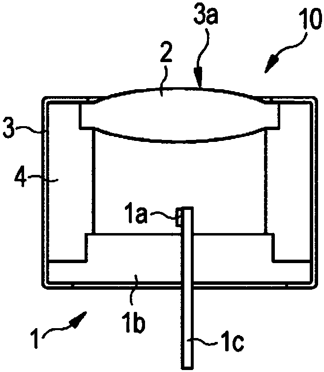
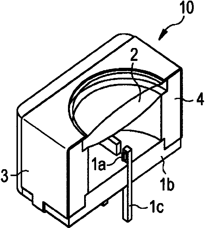
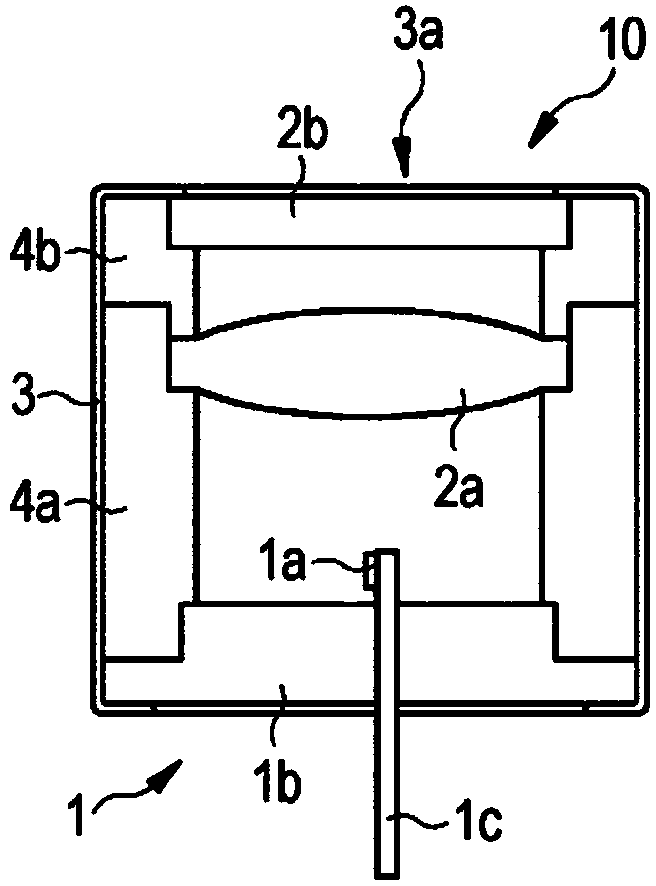
[0040] exist Figure 1A A radiation-emitting device 10 comprising an optoelectronic semiconductor component 1 and an optical element 2 is shown in . The semiconductor component 1 has a radiation-emitting semiconductor chip 1a, a housing preform 1b and a printed circuit board for electrically contacting the semiconductor chip. The semiconductor chip 1a is, for example, an LED or a laser. The circuit board 1c is used for external electrical contacting of the semiconductor chip 1a. The housing 1b partially surrounds the circuit board 1c. In particular, the ...


PUM


Abstract

A radiation-emitting device (10) is provided which includes an optoelectronic semi-conductor element (1) and at least one optical element (2, 2a, 2b). The optical element (2, 2a, 2b) is disposed downstream of the semi-conductor device (1) in the radiation direction. The optical element (2a, 2b, 2) is mechanically attached to the semi-conductor device (1) with a bracket (3). In addition, a method is provided for producing a device (10) of this type.

Description

technical field [0001] The invention relates to a radiation-emitting device having a semiconductor component and an optical element. Furthermore, the invention relates to a manufacturing method for such a device. Background technique [0002] In the combination of the optoelectronic semiconductor component and optical elements arranged downstream, such as lenses or filters, different materials are used for the individual components, such as plastics and metals. Adhesives that reliably connect the different materials under extreme environmental conditions, for example extreme temperatures and / or humidity, are not always available here. In particular, the different coefficients of thermal expansion of the different materials of the individual components can stress the adhesive-containing connection. Furthermore, outgassing from the adhesive can negatively affect the service life of such a device or of individual components of a device. When combining different components, d...

Claims


Application Information

Patent Timeline
Patent Type & Authority Applications(China)
IPC IPC(8): G02B6/42G02B17/08H01L33/48H01S5/022
CPCG02B6/4204H01L33/483H01L33/58H01S5/02212G02B19/0061H01L2924/0002F21K9/60H01S5/02253H01L2924/00F21K9/90F21V17/06
Inventor 卡斯滕·奥恩
Owner OSRAM OPTO SEMICONDUCTORS GMBH
Why Eureka
Try Eureka