High resolution display architecture

A high-resolution, structured technology for static indicators, semiconductor/solid-state device manufacturing, instrumentation, and more to address issues such as wasted power

Active Publication Date: 2014-12-31
IGNIS INNOVATION
View PDF7 Cites 7 Cited by
  • Summary
  • Abstract
  • Description
  • Claims
  • Application Information

AI Technical Summary

Problems solved by technology

Filtering each color wastes a lot of power because much of the light energy generated is simply filtered out while only a small portion is transmitted to contribute to the displayed color content

Method used


Image

  • High resolution display architecture
  • High resolution display architecture
  • High resolution display architecture

Examples


Embodiment Construction

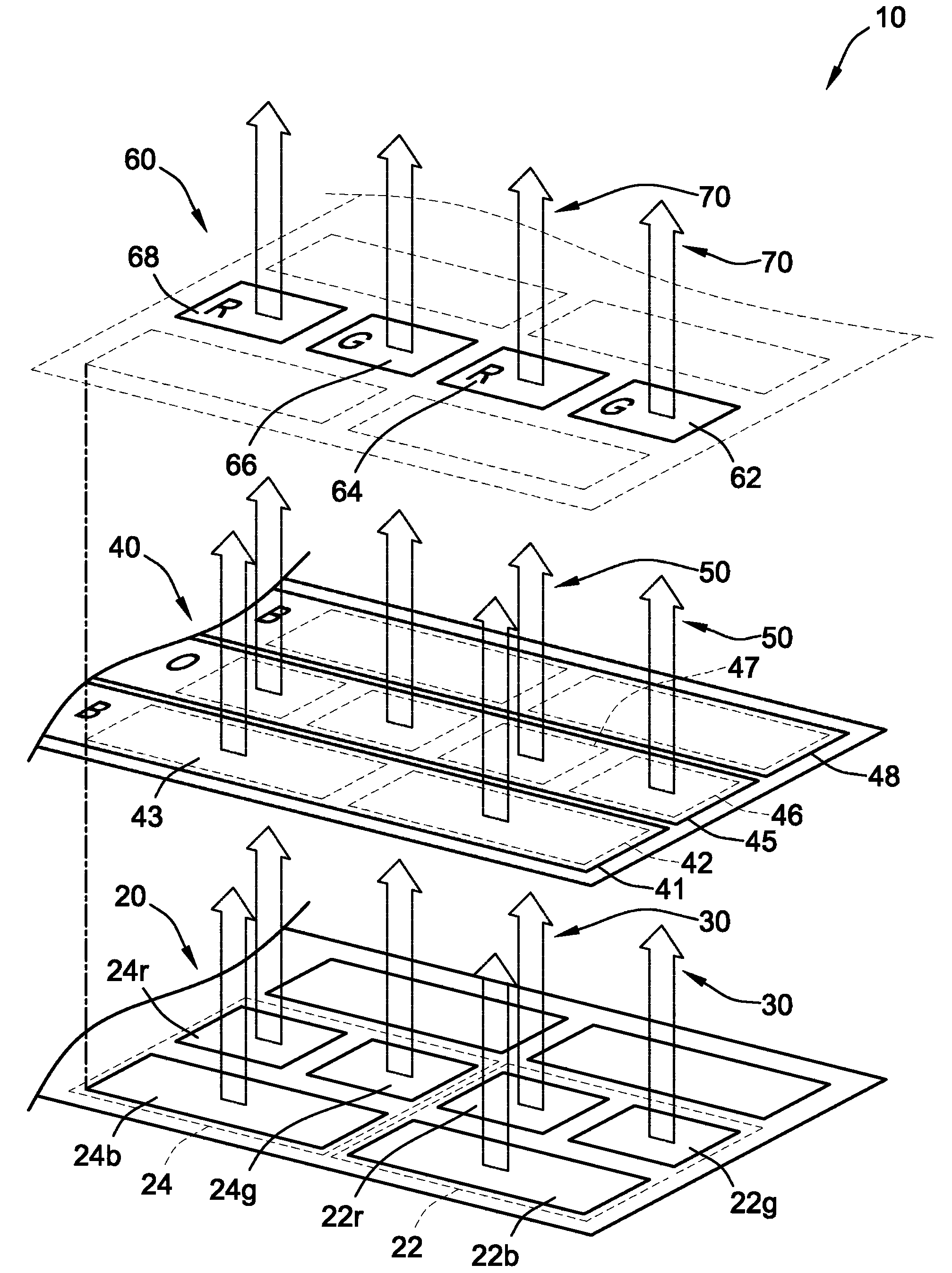
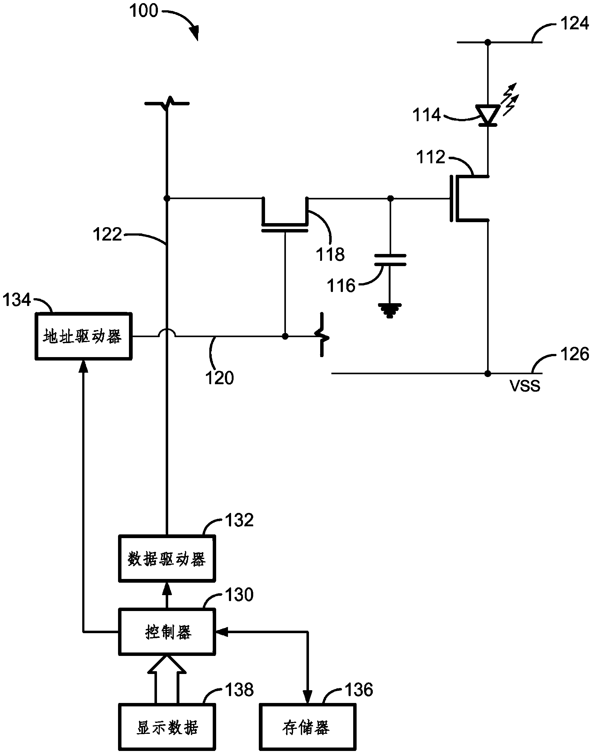
[0031] Figure 1A This is an exploded view of the display panel 10. The display panel 10 has a pattern of a TFT backplane 20 and a color filter 60. The TFT backplane 20 has an electrode array for driving current through at least one organic light-emitting layer 40. The color filter 60 The pattern is used to partially block the light 50 from the light emitting layer 40. The TFT backplane 20 can be formed on a substrate and includes a pixel circuit array for receiving programming information and delivering a driving current 30 through the light emitting layer 40. Generally, the TFT backplane 20 includes an array of electrodes (for example, electrodes 22r, 22g, 22b, etc.) arranged in rows and columns, and each electrode is associated with a different pixel circuit. The electrodes drive current through the light-emitting layer 40.

[0032] Generally, the TFT backplane is an active matrix backplane and each pixel circuit in the TFT backplane includes a driving transistor and a storage...


PUM


Abstract

An arrangement for a high resolution active matrix display includes organic emissive layers of distinct colors each deposited across continuous regions so as to include more than one pixel emissive region. Color filters are situated to partially block light from at least some of the emissive regions such that primary additive colors are transmitted from distinct subsets of pixels. The emissive layers may be deposited in alternating parallel stripes along rows or columns of the display, or may be oriented perpendicularly with respect to one another such that the emissive layers overlap in the emissive regions of at least some pixels. In some examples, red, green, and blue of pixels are arranged in regular patterns across the display and with the emissive regions for the blue pixels forming a relatively larger area of the display than either the red or green pixels.

Description

Technical field [0001] The present invention generally relates to flat panel displays formed by controllably depositing materials on a substrate, and systems and methods for manufacturing such displays, and more particularly to a light-emitting layer in which a light-emitting layer is formed by a shadow mask. An organic light emitting diode display deposited on a display substrate. Background technique [0002] Displays can be created using an array of organic light emitting devices ("OLED": organic light emitting devices), each of which is controlled by a separate circuit (ie, pixel circuit), the circuit having the following transistors : This transistor is used to selectively control the circuit so that the circuit is programmed using the display information and emits light corresponding to the display information. Thin film transistors ("TFT": Thin film transistors) prepared on a substrate can be incorporated into such pixel circuits. [0003] Generally, such a pixel circuit i...

Claims


Application Information

Patent Timeline
Patent Type & Authority Applications(China)
IPC IPC(8): H01L21/98G09F9/33G09G3/32H01L25/16H01L51/50H05B44/00
CPCH10K59/351H10K59/352H10K59/38H10K59/32H10K59/353
Inventor 戈尔拉玛瑞扎·恰吉
Owner IGNIS INNOVATION
Why Eureka
Try Eureka