Nonvolatile semiconductor memory device

A storage device, non-volatile technology, applied in the field of non-volatile semiconductor storage devices, can solve problems such as data changes, and achieve the effect of high data retention characteristics

Active Publication Date: 2015-01-14
KIOXIA CORP +1
View PDF4 Cites 7 Cited by
  • Summary
  • Abstract
  • Description
  • Claims
  • Application Information

AI Technical Summary

Problems solved by technology

[0006] But a problem arises: if the ion-conductive memory is placed in an environment such as a room, the formed filaments will gradually change, and thus the stored data will also change.

Method used


Image

  • Nonvolatile semiconductor memory device
  • Nonvolatile semiconductor memory device
  • Nonvolatile semiconductor memory device

Examples


no. 1 example

[0026] First, the overall configuration of the nonvolatile semiconductor memory device according to the first embodiment will be described.

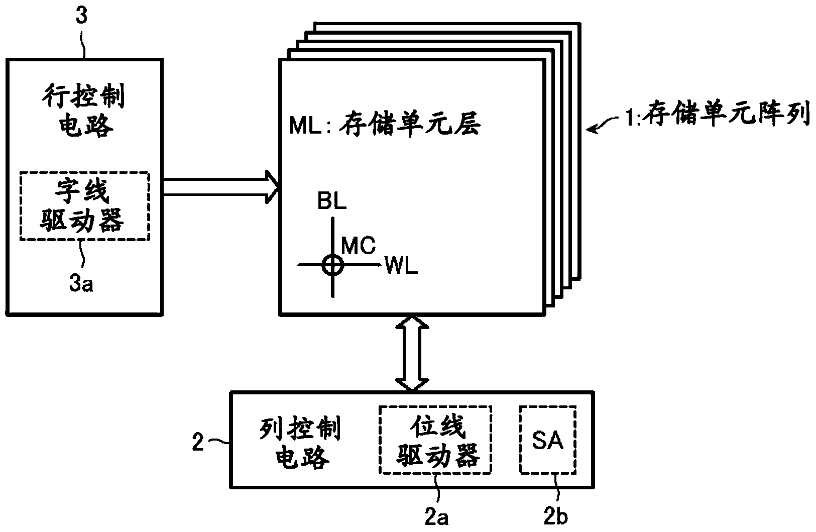
[0027] figure 1 is a block diagram showing the overall configuration of the nonvolatile semiconductor memory device according to the present embodiment.

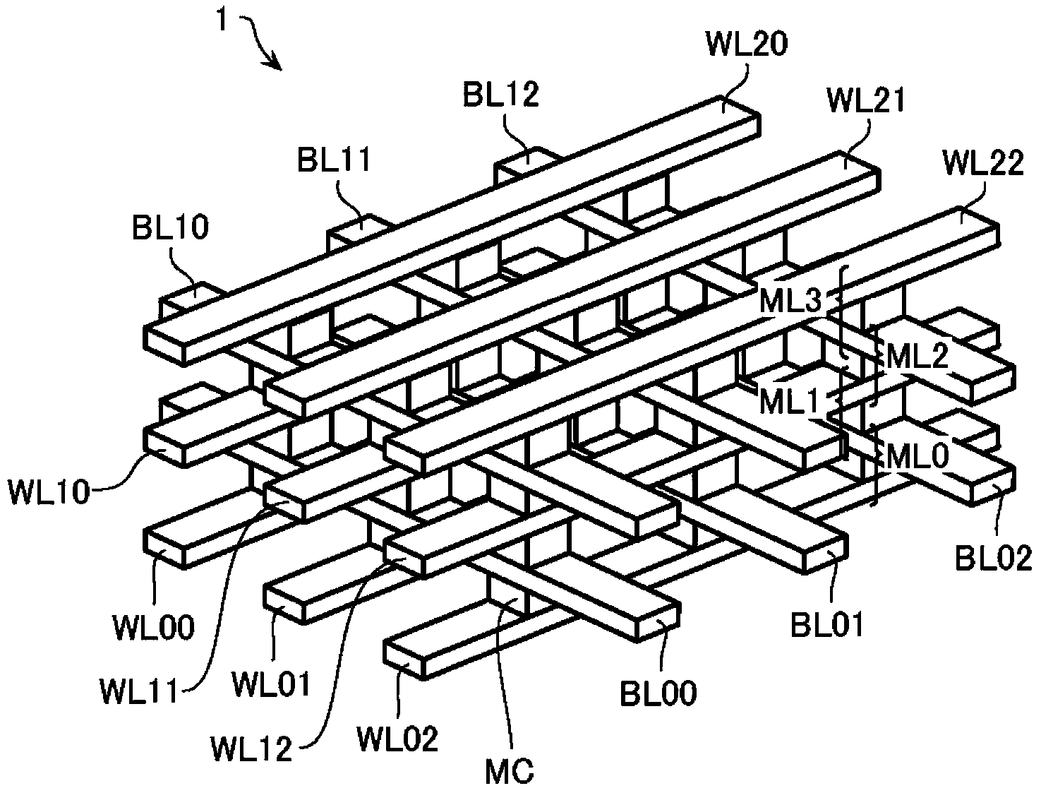
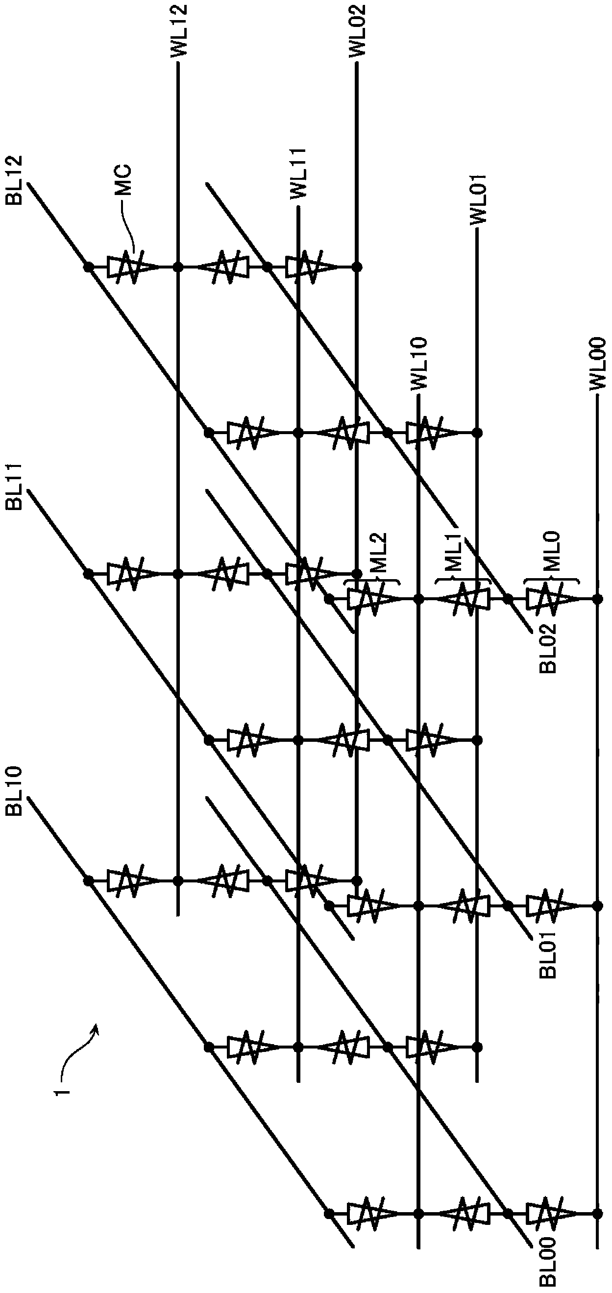
[0028] The nonvolatile semiconductor memory device includes a memory cell array 1 , a column control circuit 2 and a row control circuit 3 that control data erasing, data writing, and data reading with respect to the memory cell array 1 . The memory cell array 1 includes a plurality of stacked memory cell layers ML. Each memory cell layer ML includes a plurality of bit lines BL (first lines) and a plurality of word lines WL (second lines) intersecting each other, and memory cells MC connected to respective intersections of these bit lines BL and word lines WL . It should be pointed out below that data erasing, data writing and data reading with respect to the memory cell array 1 or ...

no. 2 example

[0076] The second embodiment describes a different writing sequence than the first embodiment.

[0077] Figure 10 is a graph showing voltages applied to memory cells during a write sequence of the nonvolatile semiconductor memory device according to the second embodiment. It should be pointed out that Figure 10 The pulse indicated by the dash / double-dot dash line in is the reset pulse ( Figure 10 Shown as "reset"), the reset pulse has the height of the reset voltage Vreset required for the reset operation. It should be noted that the reset pulse is indicated for reference and is not actually applied to the memory cell MC during the write sequence.

[0078] First, in step S201, a removal step is performed. This removal step is similar to that in step S103 in the first embodiment. As a result, only weakly coupled metal atoms included in the fibrils that have been formed by the previous writing sequence or the like are pulled back to the metal layer 11 .

[0079] Then, i...

no. 3 example

[0085] The third embodiment describes a writing sequence different from that of the first and second embodiments.

[0086] Figure 11 is a diagram showing voltages applied to memory cells during a write sequence of the nonvolatile semiconductor memory device according to the third embodiment. It should be pointed out that Figure 11 The pulse indicated by the dash / double-dot dash line in is the reset pulse ( Figure 11 Shown as "reset"), the reset pulse has the height of the reset voltage Vreset required for the reset operation. It should be noted that the reset pulse is indicated for reference and is not actually applied to the memory cell MC during the write sequence.

[0087] First, in step S301, a setting step is performed. This setting step is similar to that in step S101 in the first embodiment. This step results in elongation of the fibrils in the ion-conducting layer 12 .

[0088] Then, in step S302, a removal step is performed. This removal step is similar to t...


PUM


Abstract

A nonvolatile semiconductor memory device according to an embodiment comprises: a memory cell array including a plurality of memory cells provided one at each of intersections of a plurality of first lines and a plurality of second lines and each storing data by a data storing state of a filament; and a control circuit configured to execute a write sequence that writes data to the memory cell, the write sequence including: a setting operation that applies a setting pulse having a first polarity to the memory cell; and a removing operation that applies a removing pulse having a second polarity opposite to the first polarity to the memory cell; and the control circuit, during execution of the write sequence, is configured to repeatedly execute the setting operation until the memory cell attains a desired data storing state, and then to execute the removing operation.

Description

[0001] Cross References to Related Applications [0002] This application is based on and claims priority from prior Japanese Patent Application No. 2013-146963 filed on July 12, 2013, the entire contents of which are hereby incorporated by reference. technical field [0003] Embodiments of the present invention relate to nonvolatile semiconductor memory devices. Background technique [0004] In recent years, resistance change memory (ReRAM: Resistive RAM) has attracted attention as a technology for achieving a higher degree of integration of semiconductor memory devices. [0005] One type of resistance change memory uses an ion-conductive memory as a memory cell (cell), and the ion-conductive memory is configured to have a metal layer and an ion-conductive layer stacked therein. When an electric signal is applied to the ion-conducting layer, metal atoms included in the metal layer are ionized and migrate within the ion-conducting layer to form filaments composed of metal a...

Claims


Application Information

Patent Timeline
Patent Type & Authority Applications(China)
IPC IPC(8): G11C16/06G11C16/14
CPCG11C13/0069G11C13/0002G11C13/0097G11C13/0004G11C13/0007G11C13/0011G11C13/0064G11C2013/0092G11C2213/71G11C2213/73
Inventor 松并绚也
Owner KIOXIA CORP
Why Eureka
Try Eureka