Radio frequency lateral double diffused field effect transistor and its manufacturing method

A field-effect transistor and lateral double-diffusion technology, which is applied in semiconductor/solid-state device manufacturing, semiconductor devices, semiconductor/solid-state device components, etc., can solve the problems of reducing the electric field intensity under the polysilicon gate and affecting the life of the device, so as to reduce the output The effect of capacitance and simple process

Active Publication Date: 2017-06-06
SHANGHAI HUAHONG GRACE SEMICON MFG CORP
View PDF6 Cites 0 Cited by
  • Summary
  • Abstract
  • Description
  • Claims
  • Application Information

AI Technical Summary

Problems solved by technology

And its hot carrier capacity (HCI) also affects the life of the device. In general, in order to improve the hot carrier injection capability of the device, a ladder gate structure is usually used to reduce the electric field intensity under the polysilicon gate.

Method used


Image

  • Radio frequency lateral double diffused field effect transistor and its manufacturing method
  • Radio frequency lateral double diffused field effect transistor and its manufacturing method
  • Radio frequency lateral double diffused field effect transistor and its manufacturing method

Examples


Embodiment 1

[0041] A method for manufacturing a radio-frequency lateral double-diffused field-effect transistor, comprising the following steps:

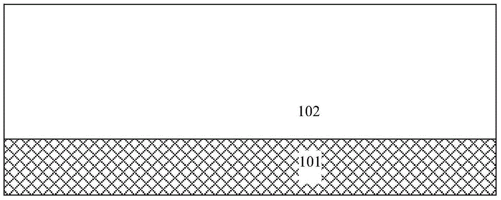
[0042] 1. grow lightly doped P-type epitaxial layer 102 on heavily doped P-type substrate 101, as figure 2 shown;

[0043] 2. growing a first oxide layer by thermal oxidation on the P-type epitaxial layer 102;

[0044]3. Keep the first oxide layer in the middle of the P-type epitaxial layer 102, and etch away all other first oxide layers on the P-type epitaxial layer;

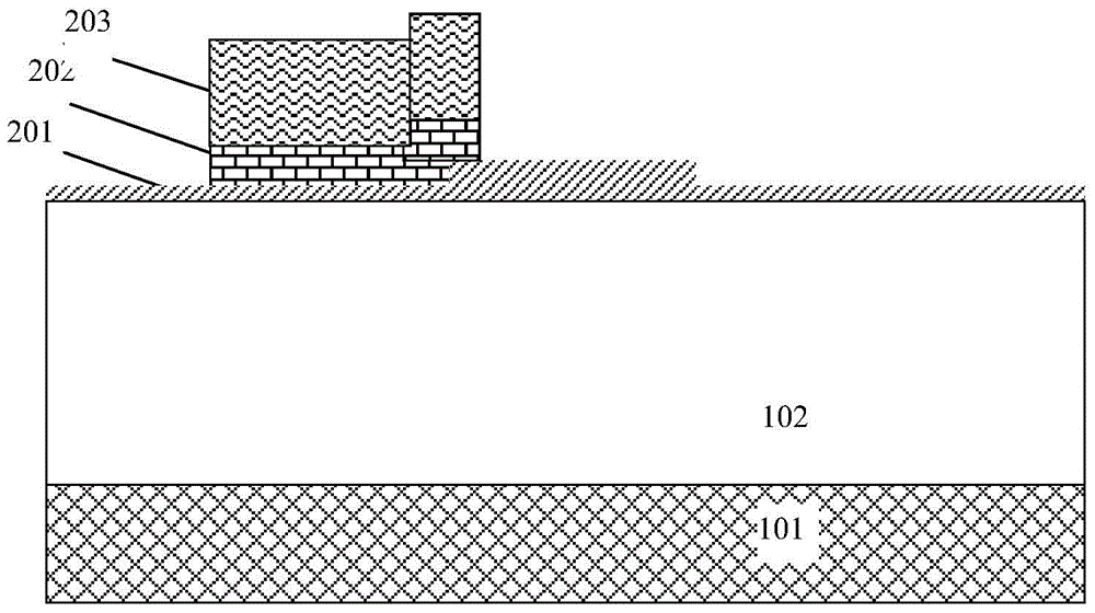
[0045] 4. On the P-type epitaxial layer 102, the second oxide layer is grown by thermal oxygen. The second oxide layer is thinner than the first oxide layer. From the left end to the right end, the structure of the oxide layer on the P-type epitaxial layer 102 is thick and thin. structure;

[0046] 5. Deposit polysilicon on the oxide layer 201, etch the polysilicon gate 202 by photolithography, the left part of the polysilicon gate covers the right end of the thin oxide laye...

Embodiment 2

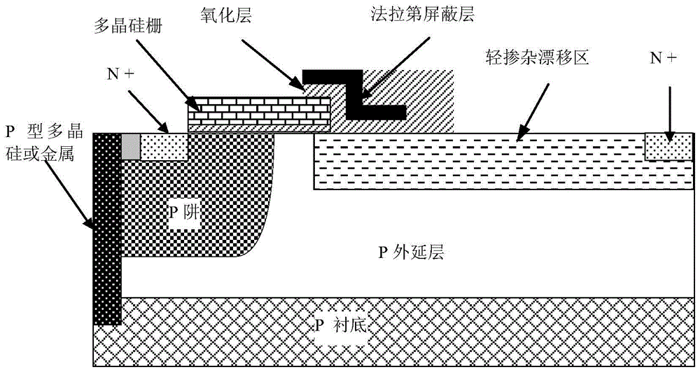
[0063] RF lateral double-diffused field-effect transistors, such as Image 6 As shown, a P-type epitaxial layer 102 is grown on a P-type substrate 101, a P-type epitaxial layer 102 is formed with a P-well 401 on the left, and an N-type drift region 301 is formed on the right. On the P-type epitaxial layer 102 between the left parts of the region 301, a stepped gate oxide and a stepped polysilicon gate 202 are sequentially formed on the left and right, and above the N-type drift region 301 adjacent to the right side of the polysilicon gate 202. A stepped Faraday shielding dielectric layer with a high left and a low right and a Faraday shielding metal 601. The stepped Faraday shielding dielectric layer is located between the stepped Faraday shielding metal layer 601 and the N-type drift region 301, and is high from left to right. There are three thickness distributions of , medium and low, the doping concentration of the N-type drift region located directly below the stepped Far...


PUM


Abstract

The invention discloses a radio frequency lateral double-diffusion field effect transistor, which has a stepped polysilicon gate and a stepped Faraday shielding layer, which not only maintains a small input capacitance, but also reduces the output capacitance and reduces the electric field intensity under the edge of the gate. The invention also discloses a method for making a radio-frequency lateral double-diffused field effect transistor. In the process of making the stepped polysilicon gate, no steps are added, and only the first layer of oxide layer is made from the source end to the drain in one etching. The end is a thin and thick structure, which can help the subsequent formation of the Faraday shielding layer to be a thick oxide layer near the polysilicon gate, and a stepped type of thin oxide layer near the drain end. The manufacture of the stepped Faraday shielding layer does not need to introduce any other process. It only needs to be formed together under the condition of forming the stepped gate oxide, and the process is simple.

Description

technical field [0001] The invention relates to semiconductor technology, in particular to a radio-frequency lateral double-diffusion field-effect transistor and a manufacturing method thereof. Background technique [0002] With the advent of the 3G era, more and more communication fields require the development of higher power RF devices. Radio Frequency Lateral Double Diffusion Field Effect Transistor (RFLDMOS), due to its very high output power, has been widely used in portable wireless base station power amplification as early as the 1990s, and its application frequency is 900MHz to 3.8GHz. Compared with traditional silicon-based bipolar transistors, RFLDMOS has better linearity, higher power and gain. Today, RFLDMOS is more popular than bipolar, and GaAs devices. [0003] The current structure of RFLDMOS is as follows figure 1 As shown, this structure has a lightly doped drift region (LDD) at the drain end, so that it has a larger breakdown voltage (BV), and at the s...

Claims


Application Information

Patent Timeline
Patent Type & Authority Patents(China)
IPC IPC(8): H01L29/78H01L29/06H01L21/336
CPCH01L23/552H01L29/42368H01L29/42376H01L29/66681H01L29/7816H01L29/1045H01L29/402H01L29/66659H01L29/7835
Inventor 李娟娟蔡莹
Owner SHANGHAI HUAHONG GRACE SEMICON MFG CORP
Why Eureka
Try Eureka