
Block-division low-power-consumption magnetic memory cache framework design method

A technology of magnetic memory and architecture design, applied in the direction of digital memory information, static memory, memory system, etc., can solve the problem of high write power consumption of on-chip cache, and achieve the effect of reducing write power consumption

Active Publication Date: 2015-02-04
BEIHANG UNIV
View PDF4 Cites 0 Cited by
  • Summary
  • Abstract
  • Description
  • Claims
  • Application Information

AI Technical Summary

Problems solved by technology

The data interaction between the on-chip cache and the processor core is the most frequent. If data needs to be frequently written to the cache during program execution, the power consumption of the on-chip cache based on STT-MRAM technology will be very large, which may offset the use of STT-MRAM. the benefits

Method used


Image

  • Block-division low-power-consumption magnetic memory cache framework design method
  • Block-division low-power-consumption magnetic memory cache framework design method
  • Block-division low-power-consumption magnetic memory cache framework design method

Examples


Embodiment Construction

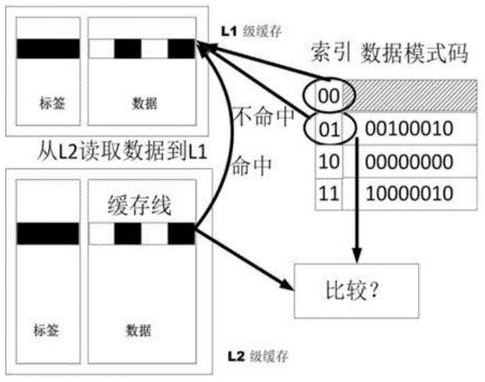
[0023] The invention aims to solve the problem of excessive writing energy consumption caused by using non-volatile memory such as STT-MRAM as an on-chip cache. By analyzing the characteristics of data written in the L1 and L2 caches, a single block in the L1 cache is divided into several sub-blocks. In addition to storing the content of the original block, each block also sets an additional index bit. The purpose of the index bit will be described later. Each sub-block has three modes: 0 (all bits in the block are 0), 1 (all bits in the block are 1), 2 (other modes that are neither 0-mode nor 1-mode). The mode is expressed in units of blocks. For example, if a block is divided into four sub-blocks, the mode of the block is composed of four sub-patterns. These four sub-patterns correspond to a sub-block respectively, and each sub-pattern is 0, 1, and 2. one of the . In this way, each block has a corresponding unique combination mode.

[0024] See figure 2 , the present inv...


PUM


Abstract

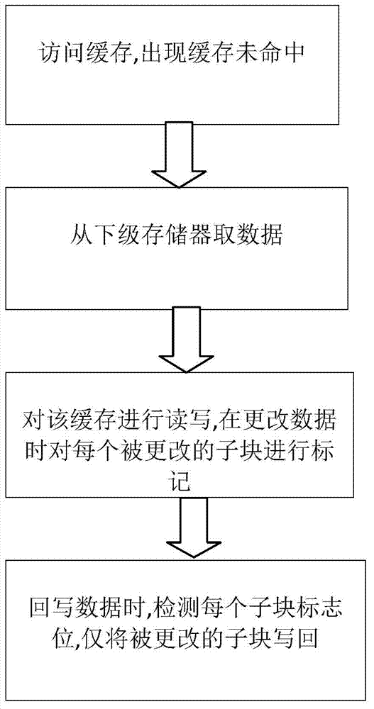
A block-division low-power-consumption magnetic memory cache architecture design method comprises four major steps: 1, a plurality of block modes with highest appearing frequency in L1 written-back data and L1 read data are subjected to statistics, then a mode table is composed, and an index value is correspondingly allocated; two, when a program runs, the pattern table is loaded to a special L1 level cache; when new data is read from an L2 level cache, a mode of the new data is calculated, and whether the mode of the new data is hit is examined in the mode table; three, when data needs to be written back to the L2 level cache, a mode of the data is again calculated, the mode is compared with a mode indicated by an index bit of a block, and a control bit is obtained; and four, when the data is written back to the L2, the control bit controls a writing operation of a corresponding sub block, if the control bit is 1, a written-back control signal of the data of the corresponding sub block is set to be valid, otherwise a writing enable of the corresponding sub block is invalid.

Description

technical field [0001] The invention relates to a low-power magnetic memory cache architecture design method for word block division. It divides the cache into sub-blocks, adds data change flag bits for the sub-blocks, and divides the sub-blocks into sub-blocks by identifying the flag bits. different categories. A magnetic memory architecture design method for reducing cache write energy consumption by optimizing write operations of different types of sub-blocks. It belongs to the technical field of magnetic memory and low power consumption design. technical background [0002] With the continuous improvement of process size, the integration level of on-chip transistors is getting higher and higher. In order to greatly improve processor performance under a given power consumption constraint, multi-core processors have begun to be widely used. As the number of cores increases, processors have greater and greater requirements for on-chip cache capacity and bandwidth. With ...

Claims


Application Information

Patent Timeline
Patent Type & Authority Applications(China)
IPC IPC(8): G11C11/16
CPCG11C11/1653G11C11/1675G06F12/0811G06F12/0844
Inventor 张小龙吴比成元庆郭玮赵巍胜
Owner BEIHANG UNIV
Learn More