
A magnetic random access memory and its writing method, reading method and preparation method

A technology of magnetic random access memory and magnetic moment direction, which is applied in static memory, digital memory information, information storage, etc., can solve the problems of large MRAM size and low storage density of MRAM, and achieve the effect of reducing energy consumption for writing

Active Publication Date: 2020-09-18
SOUTH UNIVERSITY OF SCIENCE AND TECHNOLOGY OF CHINA
View PDF5 Cites 0 Cited by
  • Summary
  • Abstract
  • Description
  • Claims
  • Application Information

AI Technical Summary

Problems solved by technology

[0004] The invention provides a magnetic random access memory (MRAM) and its writing method, reading method and preparation method, which solves the problem of relatively wide MRAM size caused by wide line width when using the induced magnetic field or polarized current of the wire to realize MRAM writing in the prior art. Large, low memory density issues with MRAM

Method used


Image

  • A magnetic random access memory and its writing method, reading method and preparation method
  • A magnetic random access memory and its writing method, reading method and preparation method
  • A magnetic random access memory and its writing method, reading method and preparation method

Examples


Embodiment 1

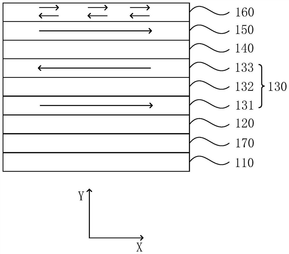
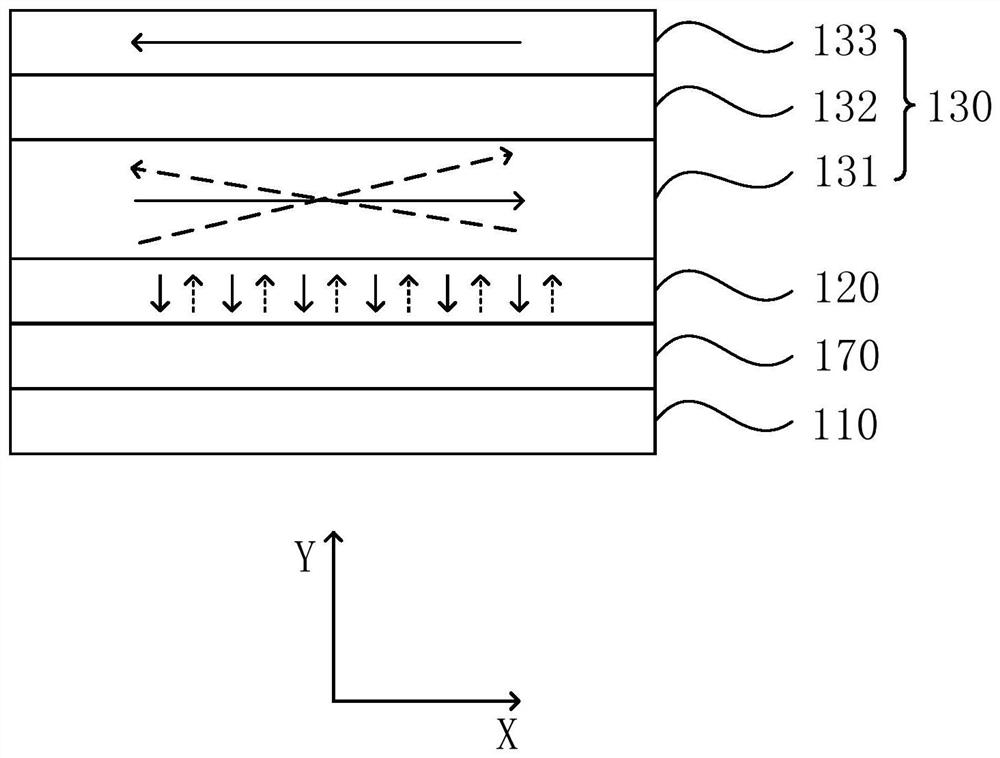
[0039] figure 1 It is a schematic structural diagram of a magnetic random access memory provided in Embodiment 1 of the present invention. see figure 1 , the MRAM includes a substrate layer 110, a ferroelectric layer 120, a composite antiferromagnetic structure 130, a first isolation layer 140, and a first ferromagnetic layer 150 stacked in sequence, and the composite antiferromagnetic structure 130 is an MRAM Free layer, the first ferromagnetic layer 150 is the fixed layer of MRAM; the ferroelectric layer 120 undergoes polarization or phase change under the action of an applied voltage, which is used to change the coupling state of the composite antiferromagnetic structure 130; the first ferromagnetic The layer 150 has a constant first magnetic moment direction; the first isolation layer is used to control the first magnetic moment direction from being affected by the coupling state of the composite antiferromagnetic structure 130 .

[0040] Exemplary, figure 1 The structu...

Embodiment 2

[0052] Figure 4 It is a schematic flowchart of a writing method of a magnetic random access memory provided in Embodiment 2 of the present invention, see Figure 4 , on the basis of Embodiment 1, the MRAM provided in this embodiment includes a substrate layer, a ferroelectric layer, a composite antiferromagnetic structure, a first isolation layer, and a first ferromagnetic layer stacked in sequence. The embodiment of the present invention The writing methods of the provided magnetic random access memory include:

[0053] S210. Obtain a write instruction of the MRAM.

[0054] Wherein, the write instruction refers to a machine instruction obtained by a control circuit connected to the magnetic random access memory, which exemplarily includes corresponding instructions such as typing characters or pasting pictures, and the acquisition path exemplarily includes using a keyboard to write, a mouse click, etc. The instruction generated corresponding to the click and the like is no...

Embodiment 3

[0063] Figure 5 It is a schematic flowchart of a method for reading a magnetic random access memory provided in Embodiment 3 of the present invention, see Figure 5 , on the basis of the above-mentioned embodiments, the MRAM provided by this embodiment includes a substrate layer, a ferroelectric layer, a composite antiferromagnetic structure, a first isolation layer and a first ferromagnetic layer that are stacked in sequence. The embodiment of the present invention The read method of the provided MRAM includes:

[0064] S310. Obtain a read instruction of the MRAM.

[0065] Wherein, the reading instruction refers to a machine instruction obtained by a control circuit connected to the magnetic random access memory, which exemplarily includes instructions corresponding to displaying characters, displaying pictures, playing audio and video, etc., and the acquisition path includes corresponding actions such as clicking the mouse Generated instructions.

[0066] S320. Apply a c...


PUM

PropertyMeasurementUnit
electrical resistanceaaaaaaaaaa
thicknessaaaaaaaaaa

Abstract

The invention discloses a magnetic random access memory and its writing method, reading method and preparation method. The magnetic random access memory comprises a substrate layer, a ferroelectric layer, a composite antiferromagnetic structure, a first isolation layer and a second A ferromagnetic layer, the composite antiferromagnetic structure is the free layer of the MRAM, the first ferromagnetic layer is the fixed layer of the MRAM; The coupling state of the composite antiferromagnetic structure; the first ferromagnetic layer has a constant first magnetic moment direction; the first isolation layer is used to control the first magnetic moment direction from being affected by the coupling state of the composite antiferromagnetic structure. This magnetic random access memory uses the mutual transformation of the ferromagnetic coupling and antiferromagnetic coupling of the compound antiferromagnetic structure under the action of an electric field to realize the writing of MRAM, and solves the problem of wires when using the induced magnetic field or polarized current of a wire to realize MRAM writing. The problem of larger MRAM size caused by wider width and lower storage density of MRAM achieves high-density storage.

Description

technical field [0001] Embodiments of the present invention relate to the field of semiconductors and storage devices, and in particular to a magnetic random access memory (MRAM) and its writing method, reading method and manufacturing method. Background technique [0002] The traditional magnetic random access memory (MRAM) consists of a free layer, an isolation layer and a fixed layer, located at the vertical intersection of the word line and the bit line; the magnetic induction effect of the current on the word line and the bit line during the writing process A magnetic field is generated to reverse the magnetization direction of the free layer; the magnetization direction of the free layer and the fixed layer are the same to achieve low magnetoresistance, and the magnetization direction is opposite to achieve high magnetoresistance. MRAM judges whether the stored data is 0 or 1 by detecting the level of magnetoresistance. Since a large current is required to reverse the...

Claims


Application Information

Patent Timeline
Patent Type & Authority Patents(China)
IPC IPC(8): H01L43/08H01L43/12G11C11/16
CPCG11C11/161H10N50/01H10N50/10
Inventor 徐泽东陈朗
Owner SOUTH UNIVERSITY OF SCIENCE AND TECHNOLOGY OF CHINA
Learn More