Diode packaging structure

A packaging structure and diode technology, applied in the direction of semiconductor/solid-state device parts, semiconductor devices, electrical components, etc., can solve the problem of poor quality of diode products, and achieve the effect of reducing the difficulty of production process, convenient connection, and strong heat dissipation performance.

Active Publication Date: 2015-02-11
CHINA ZHENHUA GRP YONGGUANG ELECTRONICS CO LTD STATE OWNED NO 873 FACTORY
View PDF3 Cites 5 Cited by
  • Summary
  • Abstract
  • Description
  • Claims
  • Application Information

AI Technical Summary

Problems solved by technology

[0002] In the existing diode packaging structure, it mainly includes a substrate, a die assembly, a package body, and leads. In a diode packaging structure with high power requirements, since the outer dimensions of the diode are fixed, the die assembly needs to be fired with a multi-layer die. Therefore, in the research and development process, not only the heat dissipation of the die, but also the connection of the electrode pads in the die assembly must be considered. Since the space formed by the substrate and the package is very small, the connection between the electrode pads and the electrodes through wires will be difficult. There is a certain degree of difficulty, and the quality of the produced diode products is likely to be poor due to the shaking of the lead wires during use

Method used


Image

  • Diode packaging structure

Examples


Embodiment Construction

[0016] The following will clearly and completely describe the technical solutions in the embodiments of the present invention with reference to the accompanying drawings in the embodiments of the present invention. Obviously, the described embodiments are only some of the embodiments of the present invention, not all of them. Based on the embodiments of the present invention, all other embodiments obtained by persons of ordinary skill in the art without creative efforts fall within the protection scope of the present invention.

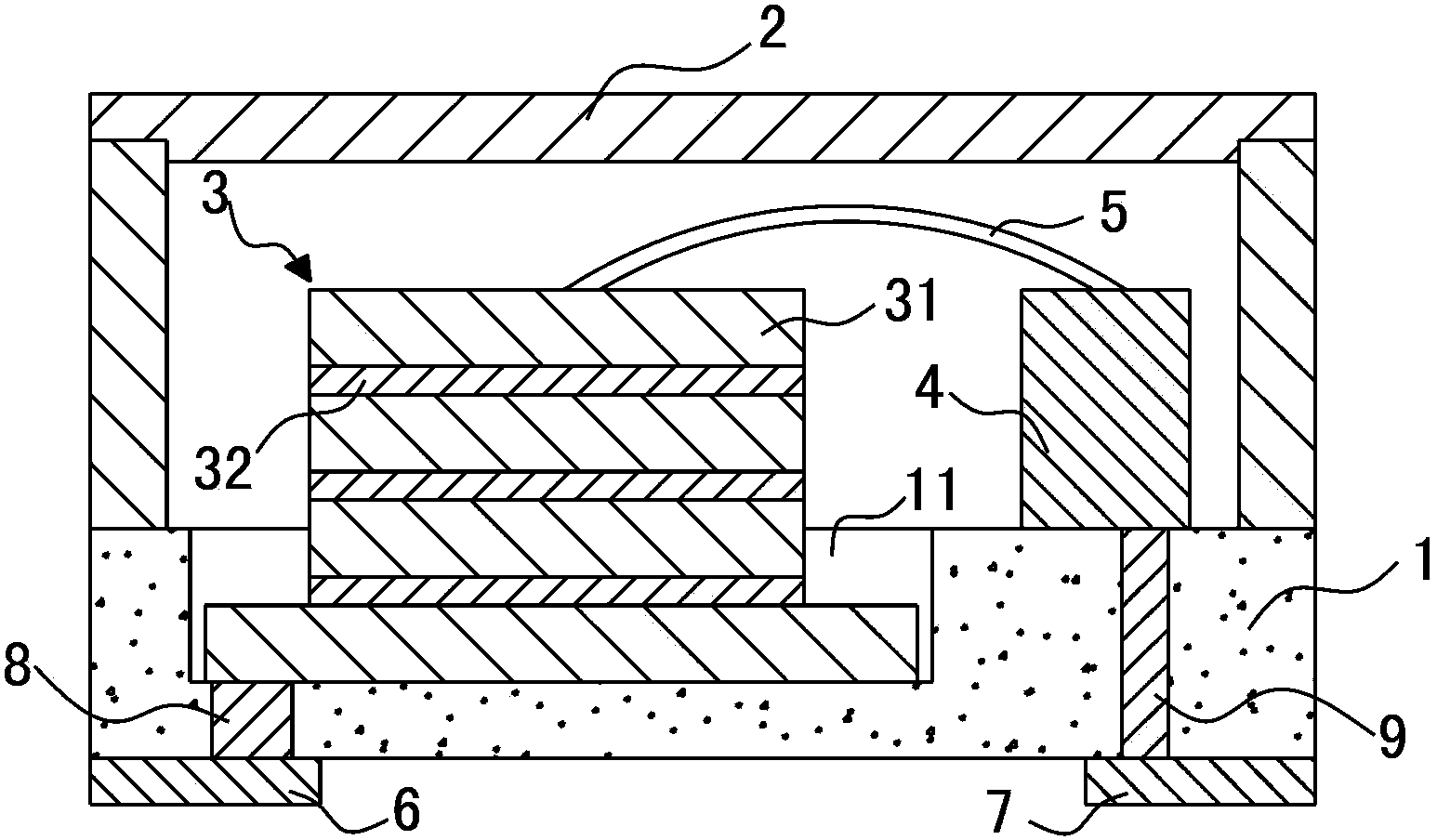
[0017] Such as figure 1 As shown, the diode packaging structure of the present invention may include a substrate 1, a package body 2 disposed on the upper end surface of the substrate 1, and several electrodes disposed on the lower end surface of the substrate 1. The upper end of the substrate 1 has a groove 11, the concave A die assembly 3 is arranged in the groove 11, and a bonding block 4 is provided on the upper surface of the substrate 1. The die...


PUM


Abstract

The invention relates to a semiconductor structure, and specifically relates to a diode packaging structure. The diode packaging structure comprises a substrate, a packaging body arranged at the upper end surface of the substrate, and a plurality of electrodes arranged at the lower end surface of the substrate. The upper end of the substrate is provided with a groove, the groove is internally provided with a tube core assembly, the upper end surface of the substrate is provided with a bonding block, the tube core assembly and the bonding block are connected through a lead wire, the packaging body and the substrate form a cavity, and the tube core assembly and the bonding block are arranged in the cavity. According to the invention, the problem of bonding between the tube core assembly and the electrodes is effectively solved, the connection between the tube core assembly and the bonding block is facilitated, the production process difficulty is lowered, the production efficiency is improved, the lead wire connecting the tube core assembly and the bonding block is not easily shaken and is not easily broken, and the quality of a manufactured product is enabled to be better. Besides, the diode packaging structure also has the advantages of good sealing performance, high heat dissipation performance and the like.

Description

technical field [0001] The invention relates to a semiconductor structure, in particular to a diode packaging structure. Background technique [0002] In the existing diode packaging structure, it mainly includes a substrate, a die assembly, a package body, and leads. In a diode packaging structure with high power requirements, since the outer dimensions of the diode are fixed, the die assembly needs to be fired with a multi-layer die. Therefore, in the research and development process, not only the heat dissipation of the die, but also the connection of the electrode pads in the die assembly must be considered. Since the space formed by the substrate and the package is very small, the connection between the electrode pads and the electrodes through wires will be difficult. There is a certain degree of difficulty, and the quality of the produced diode product is likely to be poor due to the shaking of the lead wire during use. Contents of the invention [0003] In view of...

Claims


Application Information

Patent Timeline
Patent Type & Authority Applications(China)
IPC IPC(8): H01L23/488H01L29/861H01L25/07
CPCH01L2224/48091H01L2224/48137H01L2224/73265H01L2924/00014
Inventor 杨启达丁小宏杨辉赵志云
Owner CHINA ZHENHUA GRP YONGGUANG ELECTRONICS CO LTD STATE OWNED NO 873 FACTORY
Why Eureka
Try Eureka