Light emitting element, manufacturing method thereof, and display device

A light-emitting element and manufacturing method technology, applied to electrical components, laser parts, lasers, etc., can solve problems such as radius shape bending, complex structure of super light-emitting diodes, and changing the direction of emitted light

Inactive Publication Date: 2015-02-11
SONY CORP
View PDF9 Cites 3 Cited by
  • Summary
  • Abstract
  • Description
  • Claims
  • Application Information

AI Technical Summary

Problems solved by technology

[0007] However, Japanese Unexamined Patent Application Publication No. 2-310975 discloses a technique having the following problem: Since the waveguide is inclined with respect to the light exit end face, the direction of emitted light is changed due to light refraction on the light exit end face
In addition, there is a problem that the radial shape of the light emitted from the light exit end face is curved (see Figure 21B )
Furtherm

Method used


Image

  • Light emitting element, manufacturing method thereof, and display device
  • Light emitting element, manufacturing method thereof, and display device
  • Light emitting element, manufacturing method thereof, and display device

Examples


example 2

[0047] 3. Example 2 (Methods of Manufacturing Light-Emitting Elements According to Second and Fourth Embodiments of the Present Invention) and the like.

[0048] [Explanation of the entire light-emitting element according to the first embodiment and the second embodiment of the present invention, the method of manufacturing the light-emitting element according to the first embodiment to the fourth embodiment of the present invention, and the display device of the present invention]

[0049] A method for manufacturing a light-emitting element according to the first embodiment or the second embodiment of the present invention is preferably implemented in the following form, wherein,

[0050] In the process (a), the first compound semiconductor layer, the active layer, the first layer of the second compound semiconductor layer, and the 2A layer of the second compound semiconductor layer, the first etch stop layer, the the 2B layer of the second compound semiconductor layer, the s...

example 1

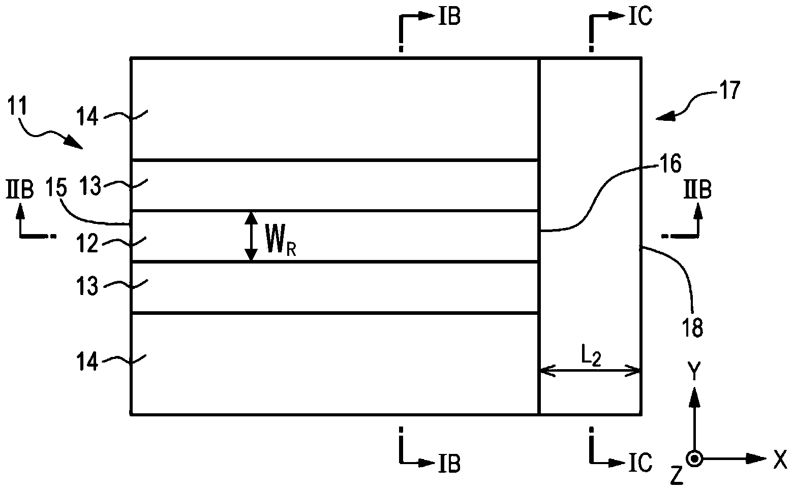
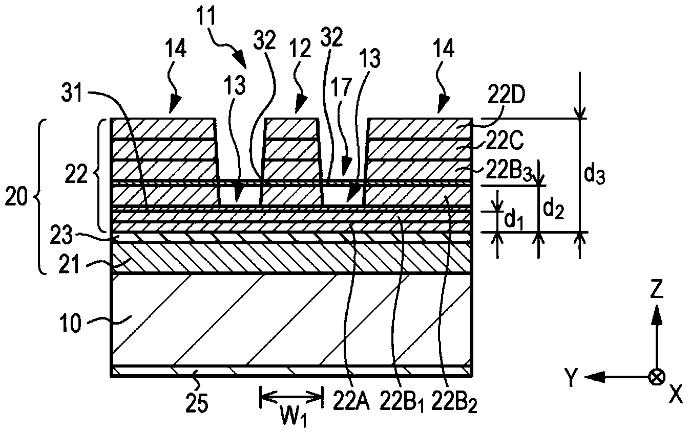
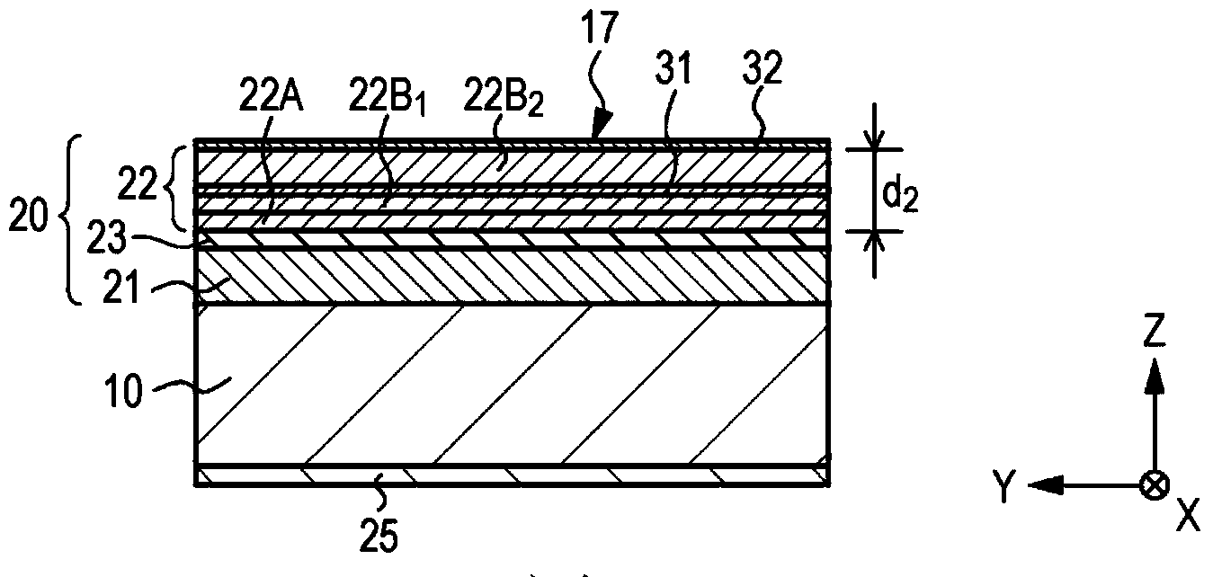
[0095] Example 1 relates to the light emitting element according to the first embodiment and the second embodiment of the present invention, and the method of manufacturing the light emitting element according to the example 1 and the third embodiment of the present invention. Figure 1A A schematic plan view showing a laminated structure constituting the light-emitting element of the first embodiment, Figure 1B showing along Figure 1A A schematic cross-sectional view of a laminated structure etc. obtained by middle arrow IB-IB, Figure 1C showing along Figure 1A A schematic cross-sectional view of a laminated structure and the like obtained by middle arrows IC-IC. also, Figure 2A A perspective view showing a laminated structure of the light-emitting element of Example 1, etc., Figure 2B showing along Figure 1A The schematic cross-sectional view of the laminated structure obtained by the middle arrow IIB-IIB, image 3 a schematic partial cross-sectional view showing...

example 3

[0147] Example 3 is a variation of Examples 1 and 2. As a schematic partial sectional view of the light propagation region 17 of the light emitting element of Example 3 Figure 9 As shown, in Example 3, the first dielectric film 24 is formed on at least one side surface of the ridge-ridge structure portion 12 and the top surface of the ridge-ridge-corrugation adjacent portion 13 (see image 3 ), and a second dielectric film 24A made of a material different from that of the first dielectric film 24 is formed on the top surface of the light propagation region 17 . Specifically, the first dielectric film 24 is made of Ta 2 o 5 made, the second dielectric film 24A is made of SiO 2 production.

[0148] The composition and structure of the light emitting element of Example 3 may be the same as those of Examples 1 and 2 except for the above-mentioned points, and thus no detailed description will be provided. As described above, by making the material of the first dielectric film ...


PUM

PropertyMeasurementUnit
Lengthaaaaaaaaaa
Lengthaaaaaaaaaa
Thicknessaaaaaaaaaa

Abstract

A light-emitting element includes a light-emitting region which is made from a stacked structure configured from a first compound semiconductor layer, an active layer, and a second compound semiconductor layer, and a light propagation region which is made from the stacked structure, extends from the light-emitting region, and has a light-emitting end surface. The light-emitting region is configured from a ridge stripe structure and ridge stripe adjacent portions positioned at both sides of the ridge stripe structure, and when a thickness of the second compound semiconductor layer in the ridge stripe adjacent portions is set to d1, a thickness of the second compound semiconductor layer in the light propagation region is set to d2, and a thickness of the second compound semiconductor layer in the ridge stripe structure is set to d3, d3>d2>d1 is satisfied.

Description

[0001] Cross References to Related Applications [0002] This application claims the benefit of Japanese Priority Patent Application JP2013-164884 filed on Aug. 8, 2013, the entire contents of which are incorporated herein by reference. technical field [0003] The present invention relates to a light emitting element, a manufacturing method thereof, and a display device including the light emitting element. Background technique [0004] For example, a so-called laser display device (ie, a display device called a projector) including a light emitting element made of a semiconductor laser element as a light source is known, for example, from Japanese Unexamined Patent Application Publication No. 2009-025462. Laser display devices are attracting attention due to their small size, light weight, and low power consumption in addition to high brightness and high definition. However, in laser display devices, speckle noise becomes a factor that degrades the image quality of images...

Claims


Application Information

Patent Timeline
IPC IPC(8): H01S5/22H01S5/028
CPCH01L33/22H01L33/0045H01L33/06H01L33/0095
Inventor 藤井贤太郎大野智辉
Owner SONY CORP
Why Eureka
Try Eureka