Unlock instant, AI-driven research and patent intelligence for your innovation.

Multi-layer circuit board and its manufacturing method

A technology of multilayer circuit board and manufacturing method, which is applied in multilayer circuit manufacturing, printed circuit manufacturing, printed circuit, etc., can solve the problems of low bonding force between conductive paste and copper foil layer, poor reliability of multilayer circuit board, etc., and achieve The effect of improving reliability

Active Publication Date: 2017-08-25
AVARY HLDG (SHENZHEN) CO LTD +1
View PDF3 Cites 0 Cited by
  • Summary
  • Abstract
  • Description
  • Claims
  • Application Information

AI Technical Summary

Problems solved by technology

In the above-mentioned manufacturing process, due to the small aperture of the formed through hole, the cross-sectional area of ​​the filled conductive paste is also relatively small, so that the contact area between the conductive paste and the copper foil layer is also small, and the conductive paste and the copper foil layer are also relatively small. The bonding force between the copper foil layers is also very small, resulting in poor reliability of the multilayer circuit board produced

Method used


Image

  • Multi-layer circuit board and its manufacturing method
  • Multi-layer circuit board and its manufacturing method
  • Multi-layer circuit board and its manufacturing method

Examples


Embodiment Construction

[0048] The circuit board provided by the technical solution and its manufacturing method will be further described in detail below in conjunction with the accompanying drawings and embodiments.

[0049] The manufacturing method of the multilayer circuit board provided by the embodiment of the technical solution includes the following steps:

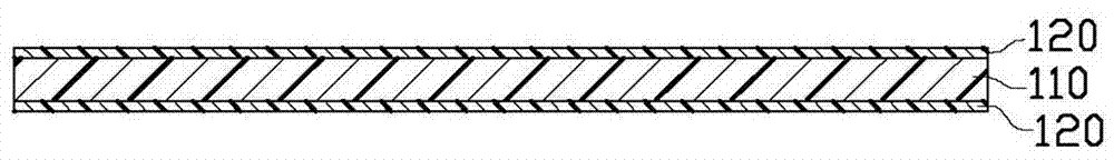
[0050] For a first step, see figure 1 , providing a plurality of insulating substrates 110 , and forming a protective layer 120 on two opposite surfaces of each insulating substrate 110 .

[0051] The insulating substrate 110 may be an epoxy resin glass fiber cloth laminated board. The protective layer can be a peelable polyethylene terephthalate (PET) film, or other peelable films.

[0052] In the second step, see figure 2 , forming a plurality of through holes 111 in each insulating base material 110 .

[0053] The multiple through holes 111 can be formed by laser ablation, and the distribution of the multiple through holes 111 can...


PUM


Abstract

The invention relates to a multi-layer circuit board, which comprises a plurality of conductive circuit layers and a plurality of insulation substrates, wherein each insulation substrate is arranged between the two adjacent conductive circuit layers, a plurality of through holes are formed in each insulation substrate, conductive paste fills each through hole, and a conductive polymer film layer is formed at the two opposite ends of the conductive paste in each through hole, and is connected between the conductive paste and the conducive circuit layers. The invention also provides a manufacturing method of the multi-layer circuit board.

Description

technical field [0001] The invention relates to circuit board manufacturing technology, in particular to a circuit board and a manufacturing method thereof. Background technique [0002] With the development of electronic products in the direction of miniaturization and high speed, circuit boards are also developing from single-sided circuit boards and double-sided circuit boards to multi-layer circuit boards. Multilayer circuit board refers to a circuit board with multiple layers of conductive lines, which has more wiring area and higher interconnection density, so it is widely used, see literature Takahashi, A.Ooki, N.Nagai, A.Akahoshi , H.Mukoh, A.Wajima, M.Res.Lab, High density multilayer printed circuitboard for HITAC M-880, IEEE Trans. on Components, Packaging, and Manufacturing Technology, 1992, 15(4):1418-1425. [0003] In the prior art, the manufacturing method of any layer full-layer via hole (ALIVH) structure multilayer circuit board generally comprises steps: pr...

Claims


Application Information

Patent Timeline
Patent Type & Authority Patents(China)
IPC IPC(8): H05K1/14H05K3/46
CPCH05K1/116H05K3/4038H05K3/429H05K3/4644H05K2201/035H05K2201/096
Inventor 覃海波郑兆孟徐茂峰黄黎明
Owner AVARY HLDG (SHENZHEN) CO LTD