Through silicon var wafer interconnection process

A technology of TSV and process, applied in the direction of electrical components, semiconductor/solid-state device manufacturing, circuits, etc., can solve the problems of high cost and complex process, and achieve the effect of low cost and reduced complexity

Inactive Publication Date: 2015-02-25
WUHAN XINXIN SEMICON MFG CO LTD
View PDF3 Cites 26 Cited by
  • Summary
  • Abstract
  • Description
  • Claims
  • Application Information

AI Technical Summary

Problems solved by technology

[0004] In order to achieve the above purpose, this application discloses a cross-wafer TSV interconnection process to so...

Method used


Image

  • Through silicon var wafer interconnection process
  • Through silicon var wafer interconnection process
  • Through silicon var wafer interconnection process

Examples


Embodiment Construction

[0026] The present invention will be further described below in conjunction with the accompanying drawings and specific embodiments, but not as a limitation of the present invention.

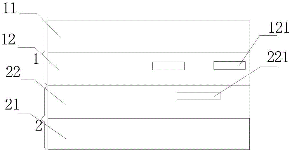
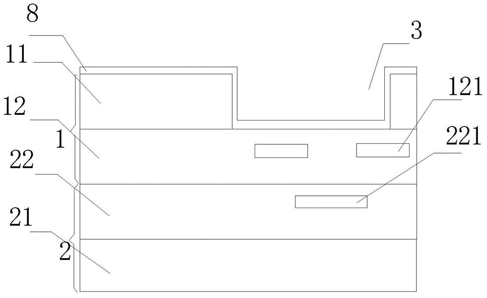
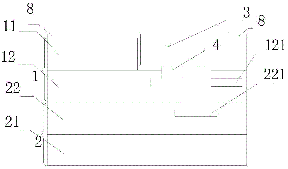
[0027] In view of the above existing problems, the present invention discloses a cross-wafer through-silicon via interconnection process, which effectively solves the need to perform three etching processes in the same area in the traditional three-dimensional integration of wafers to lead out circuits on different wafers in the same area. complex and high-cost problems, the present invention first bonds two wafers to be processed according to the traditional process and thins the first silicon substrate layer 11, and then firstly thins the thinned silicon substrate layer 11 in the same area through two etching processes. The first silicon substrate layer 21 is opened, and the film above the first metal layer is continued to be opened. At the same time, the film above the second metal layer is op...


PUM


Abstract

The invention relates to the technical field of semi-conductor manufacturing, in particular to a through silicon var wafer interconnection process. First, a first wafer and a second wafer are bonded together, a first silicon substrate layer which is thinned through etching process carried out for the first time is opened, a film on the upper side of a first metal layer is opened through the etching process carried out for the second time, and a film on the upper side of a second metal layer is opened with the first metal layer as a blocking layer, so that a groove which allows the first metal layer and the second metal layer to be both exposed is formed; the groove and openings are filled with metal, the upper surface of the metal and the upper surface of the first silicon substrate layer are covered with protective layers, and accordingly three-dimensional integration of the wafers is achieved. The through silicon var wafer interconnection process overcomes the defect that the etching process needs to be carried out three times in a traditional wafer three-dimensional integration method before circuits on different wafers on the same area are led out for circuit interconnection.

Description

technical field [0001] The invention relates to the technical field of semiconductor manufacturing, in particular to a wafer cross-silicon via interconnection process. Background technique [0002] With the miniaturization and thinning of electronic devices and memories, there are higher requirements for the volume and thickness of chips. In the prior art, completing the three-dimensional integration of wafers through through silicon vias (TSV for short) is an effective solution to reduce the size and thickness of chips. This technology integrates two or more chips with the same or different functions through Bonding integration, this integration improves the performance of the chip on a large scale while maintaining the chip volume, is no longer limited by the manufacturing process of a single chip, and also shortens the metal interconnection between functional chips, making heat generation, power consumption, The delay is greatly reduced; at the same time, the bandwidth b...

Claims


Application Information

Patent Timeline
IPC IPC(8): H01L21/768
Inventor 董金文朱继锋肖胜安胡思平
Owner WUHAN XINXIN SEMICON MFG CO LTD
Why Eureka
Try Eureka