
Memorizer address mapping method and memorizer address mapping system

A technology of memory address and mapping method, which is applied in the field of memory address mapping method, memory address mapping and system, can solve problems such as decreased access efficiency, and achieve the effect of improving access efficiency

Active Publication Date: 2015-03-11
TECHTOTOP MICROELECTRONICS
View PDF6 Cites 3 Cited by
  • Summary
  • Abstract
  • Description
  • Claims
  • Application Information

AI Technical Summary

Problems solved by technology

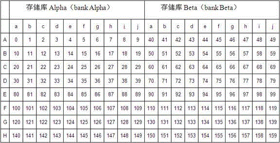
In case 1, since two accesses occur consecutively, the access operation to row 18 of storage bank A must wait for storage bank A to complete the switching action before proceeding, resulting in a significant drop in access efficiency

Method used


Image

  • Memorizer address mapping method and memorizer address mapping system
  • Memorizer address mapping method and memorizer address mapping system
  • Memorizer address mapping method and memorizer address mapping system

Examples


Embodiment Construction

[0021] Since different hosts have different functions, the lengths of continuous addresses to be accessed are different, and the access methods are also different. For example, the main function of the central processing unit (CPU) is to execute program instructions. Due to the existence of a large number of cyclic programs, the access method of the CPU to the memory device is usually to store / fetch operations on small consecutive address intervals cyclically, and the data volume is small and repeated. The following This method is called method A. In contrast, devices such as graphics processing units (GPUs) and direct memory access devices (DMAs) mainly access memory devices by one-time storage / retrieval of large continuous address ranges. The amount of data is large and one-time, as follows This method is referred to as method B.

[0022] For hosts such as the central processing unit (CPU) that need to store / retrieve small segments of continuous address ranges cyclically (m...


PUM


Abstract

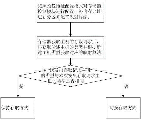
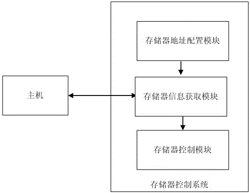
A memorizer address mapping method comprises the steps of configuring a memorizer control module according to a preset address configuration mode, partitioning a memory address and configuring mapping algorithms; configuring different address sub-partitions for different types of mainframes in the preset address configuration mode; enabling a memorizer to obtain access requests of the mainframes; obtaining the types of the mainframes and obtaining the mapping algorithms corresponding to the types of the mainframes; obtaining the types of the mainframes sending out the access requests the last time; control the memorizer to switch an access mode by means of the mapping algorithms if the types of the mainframes sending out the access requests this time are different. By means of the memorizer address mapping method, a memorizer address mapping control function is added for the memorizer, the whole memory area is divided into a plurality of sub-partitions, different characteristics of address intervals fixedly accessed by different mainframes are utilized to conduct personalized address mapping configuration on different memory sub-intervals, and the accessing efficiency of the different mainframes can be improved. In addition, the invention further provides a memorizer address mapping system.

Description

technical field [0001] The invention relates to the field of memory data processing, in particular to a memory address mapping method, memory address mapping and system. Background technique [0002] Computer systems typically include one or more Dynamic Random Access Memory (DRAM) devices, common types include but are not limited to Synchronous Dynamic Random Access Memory (SDRAM) and Double Rate Synchronous Dynamic Random Access Memory (DDR SDRAM). Under the existing DRAM architecture, the device usually consists of multiple storage banks (banks), and each storage bank (bank) usually consists of multiple storage particles. Inside the storage library, the data in the storage particle array is retrieved by using the row address (row) and the column address (column). [0003] All memory banks (banks) share multiple access control signal lines and multiple data signal lines, and it is not possible to perform deposit / retrieval operations on multiple memory banks (banks) at the...

Claims


Application Information

Patent Timeline
Patent Type & Authority Applications(China)
IPC IPC(8): G06F12/02
Inventor 王名为潘邦淦
Owner TECHTOTOP MICROELECTRONICS
Learn More