Thin-film transistor, preparation method of thin-film transistor, array substrate and display device

A thin-film transistor and thin-film technology, applied in transistors, semiconductor/solid-state device manufacturing, semiconductor devices, etc., can solve the problems of destroying the performance of the active layer and affecting the performance of thin-film transistors, so as to avoid direct damage and ensure performance.

Inactive Publication Date: 2015-03-11
BOE TECH GRP CO LTD
View PDF4 Cites 1 Cited by
  • Summary
  • Abstract
  • Description
  • Claims
  • Application Information

AI Technical Summary

Problems solved by technology

[0005] In view of this, an embodiment of the present invention provides a thin film transistor, its manufacturing method, an array substrate and a display device, to solve the problems existing in the prior art in removing the photoresist layer remaining on the active layer. When processing, it will directly destroy the performance of the active layer, thereby affecting the performance of the thin film transistor

Method used


Image

  • Thin-film transistor, preparation method of thin-film transistor, array substrate and display device
  • Thin-film transistor, preparation method of thin-film transistor, array substrate and display device
  • Thin-film transistor, preparation method of thin-film transistor, array substrate and display device

Examples


preparation example Construction

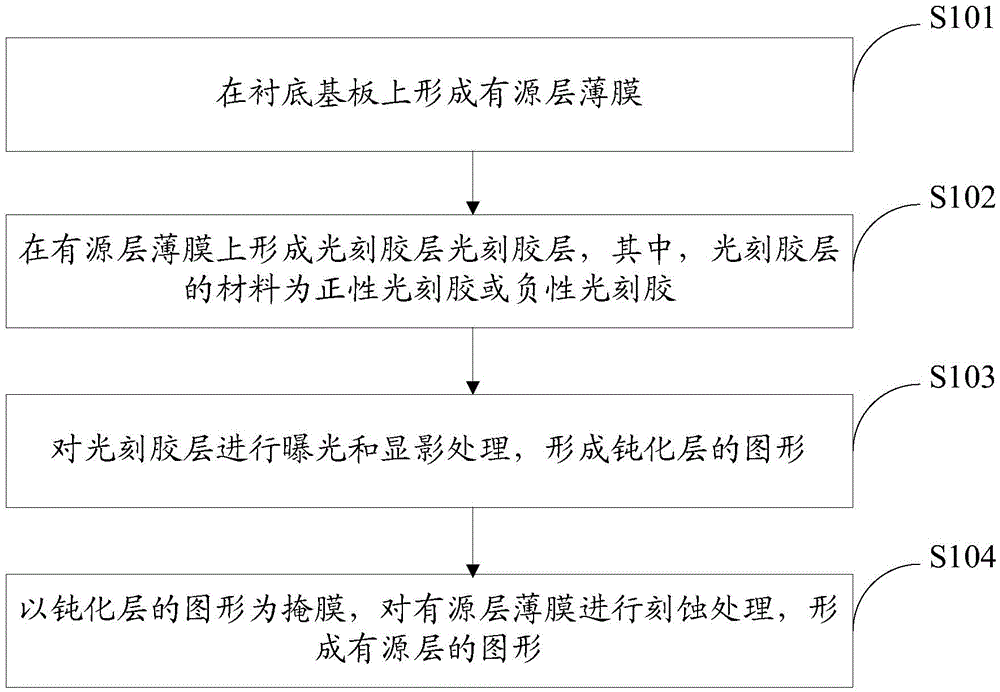
[0042] A method for manufacturing a thin film transistor provided by an embodiment of the present invention includes forming patterns of a gate electrode, a source electrode, and a drain electrode on a base substrate, and further includes:

[0043] Forming the pattern of the active layer and the pattern of the passivation layer covering the active layer through a patterning process; wherein,

[0044] The material of the passivation layer is negative photoresist or positive photoresist, the active layer and the gate electrode are insulated from each other, and the active layer is electrically connected to the source electrode and the drain electrode respectively.

[0045] In the above-mentioned preparation method provided by the embodiment of the present invention, since the material of the passivation layer is a negative photoresist or a positive photoresist, the pattern of the active layer and the passivation layer covering the active layer are formed through a patterning proc...

example 1

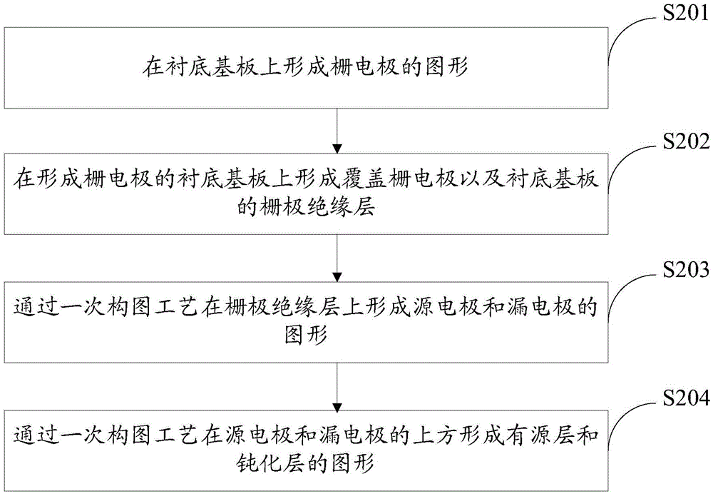
[0076] A thin-film transistor with a bottom-gate structure is prepared, which specifically includes the following steps:

[0077] (1) Form the pattern of the gate electrode 01 on the base substrate 1, such as Figure 4a shown;

[0078] Specifically, during specific implementation, a gate electrode layer may be formed on the substrate by means of thermal evaporation or sputtering, and then a pattern of the gate electrode may be formed by a photolithography process, which is not limited herein.

[0079] (2) Form a gate insulating layer 02 covering the gate electrode 01 and the base substrate 1 on the base substrate 1 on which the gate electrode 01 is formed, such as Figure 4b shown;

[0080] Specifically, in actual implementation, the gate insulating layer may be formed by evaporation, sputtering or spin coating, which is not limited herein.

[0081] (3) Form the patterns of the source electrode 03 and the drain electrode 04 on the gate insulating layer 02 through a patterni...

example 2

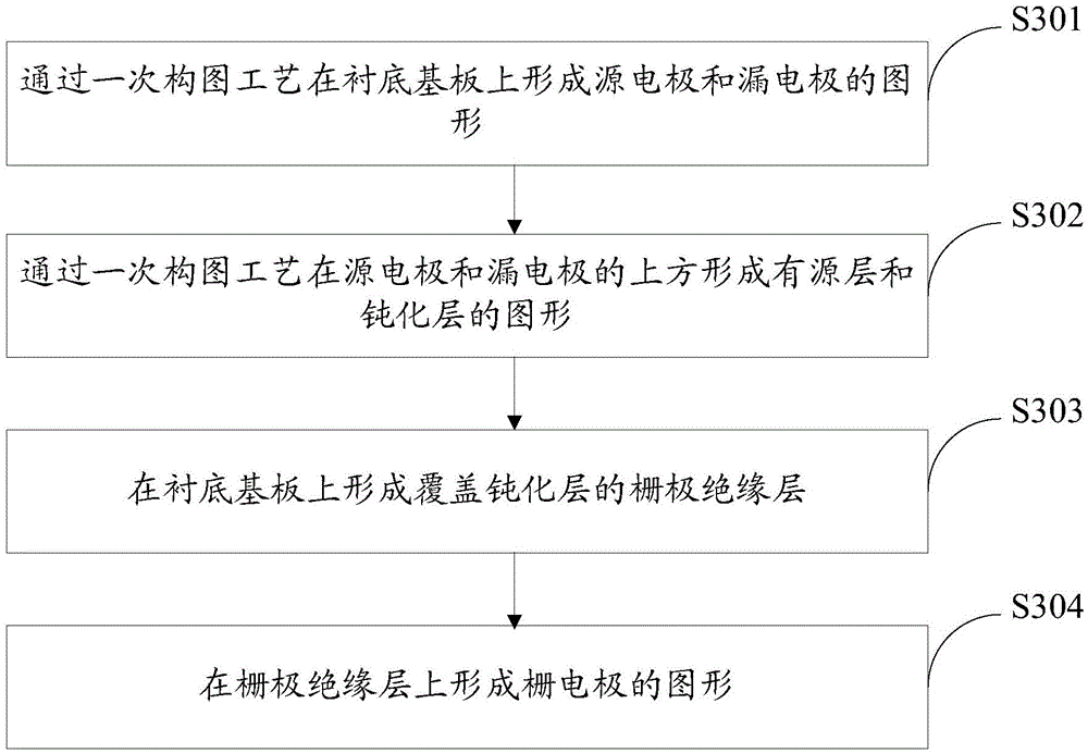
[0095] A thin film transistor with a top-gate structure is prepared, specifically comprising the following steps:

[0096] (1) Form the patterns of the source electrode 03 and the drain electrode 04 on the base substrate 1 through a patterning process, such as Figure 5a shown;

[0097] Specifically, in a specific implementation, the source and drain electrode layers may be formed on the base substrate by means of evaporation, spin coating or sputtering, and then the pattern of the source electrode and the drain electrode is formed by a photolithography process, which is not limited herein.

[0098] (2) Form the active layer film 05 above the source electrode 03 and the drain electrode 04, such as Figure 5b shown;

[0099] Specifically, during specific implementation, the thin film of the active layer may be formed by spin coating, which is not limited herein.

[0100] (3) a photoresist layer 06 with a negative photoresist material is formed on the active layer film 05, su...


PUM


Abstract

The invention discloses a thin-film transistor, a preparation method of the thin-film transistor, an array substrate and a display device. A passivation layer is made of negative photoresist or positive photoresist, so that when a graph of an active layer and a graph of the passivation layer covering the active layer are formed with a one-time composition technology, the passivation layer can be used as the photoresist for preparing the graph of the active layer, and photoresist removal treatment is not performed on the passivation layer, which is made of the negative photoresist or positive photoresist, remaining on the active layer after composition. Thus, compared with the prior art, the thin-film transistor has the advantages that direct damage to the performance of the active layer in the photoresist removal process can be avoided, and the performance of the thin-film transistor is guaranteed. In addition, the reserved passivation layer can be used as a protective layer of the active layer to prevent impurities from entering the active layer from the upper side of the active layer, and the performance of the thin-film transistor is further guaranteed.

Description

technical field [0001] The invention relates to the technical field of semiconductors, in particular to a thin film transistor, a preparation method thereof, an array substrate and a display device. Background technique [0002] Organic thin film transistor (OTFT) is a logic unit device using organic semiconductor as the active layer. It has the advantages of being suitable for large-area processing, flexible substrates, and low process cost. It is used in flat panel displays, sensors, memory cards, and radio frequency identification tags. Show application prospects. Therefore, the research and development of organic thin film transistors have received extensive attention internationally. [0003] At present, the patterning process of traditional organic thin film transistors is generally realized by inkjet printing or photolithography technology. However, the inkjet printing method can only meet the application of low pixels, and requires a new printing production equipme...

Claims


Application Information

Patent Timeline
Patent Type & Authority Applications(China)
IPC IPC(8): H01L21/336H01L21/28H01L29/786H01L29/423
CPCH01L27/1214H10K71/00H10K10/46H10K71/233H10K10/486H10K10/464H10K10/466
Inventor 谢应涛欧阳世宏蔡述澄石强刘则方汉铿
Owner BOE TECH GRP CO LTD
Why Eureka
Try Eureka