Wafer laminating device

A film sticking device and wafer technology, applied in transportation and packaging, conveyor objects, electrical components, etc., can solve the problems of film size smaller than wafer, material waste, etc., to achieve improved film sticking effect, wide application range, and strong adaptability Effect

Inactive Publication Date: 2015-03-11
上海技美科技股份有限公司
View PDF8 Cites 5 Cited by
  • Summary
  • Abstract
  • Description
  • Claims
  • Application Information

AI Technical Summary

Problems solved by technology

However, due to the existing film attachment method, the film can only be attached first before cutting the film, and the size of the attached film cannot be smaller than the wafer. The width and length of the film must be greater than the diameter of the wafer, resulting in a large waste of materials.

Method used


Image

  • Wafer laminating device
  • Wafer laminating device
  • Wafer laminating device

Examples


Embodiment 1

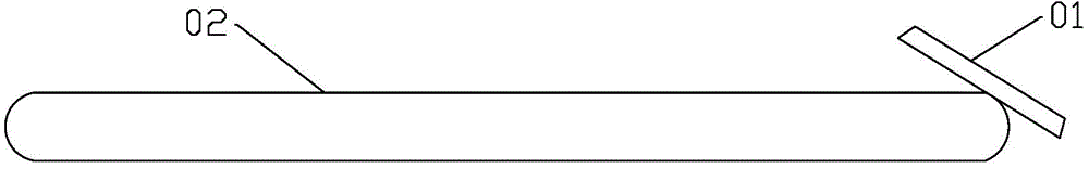
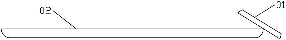
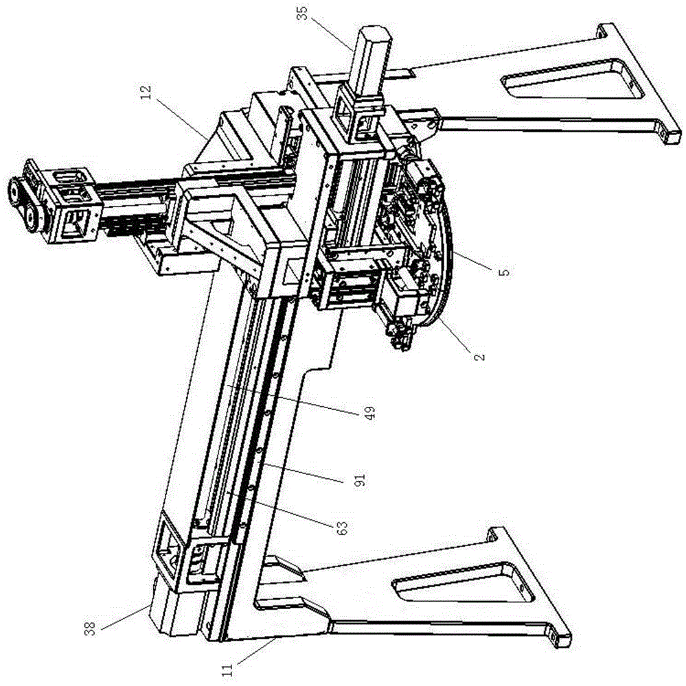
[0054] Such as Figure 3-13 As shown, the wafer attaching device includes a support frame 11 and a support arm 12 . The support arm 12 is mounted on the support frame 11 so as to move left and right. A first bracket 13 is also included, and the first bracket 13 is installed on the support arm 12 in a liftable manner. A second bracket 14 is also included, and the second bracket 14 is mounted on the first bracket 13 so that it can move left and right.

[0055] The wafer attaching device also includes a first fixing device 2 . The first fixing device 2 includes a first adsorption plate 21 . The first adsorption plate 21 is reversibly mounted on the first bracket 13 via the first rotating shaft 22 . The first adsorption plate 21 tilts after turning over. A first driving device is installed on the first support 13 , and the first driving device is a first air cylinder 31 . The first cylinder 31 drives the first adsorption plate 21 to turn over through the first transmission d...

Embodiment 2

[0084] Different from Embodiment 1, the wafer attaching device in this embodiment does not include the first clamping plate 23 and the second clamping plate 53, and only absorbs the film through the first adsorption plate 21 and the second adsorption plate 51, and also It can achieve the clamping function of the film.


PUM


Abstract

The invention discloses a wafer laminating device. The wafer laminating device is characterized by comprising a first fixing device, a second fixing device and a pressing device, wherein the first fixing device is arranged in such a manner that the first fixing device can move leftwards and rightwards; the second fixing device is arranged in such a manner that the second fixing device can move leftwards and rightwards; the second fixing device and the first fixing device get close to and far away from each other when either or both of the second fixing device and the first fixing device move; the first device and the second device are used together for clamping a film; the pressing device is arranged in such a manner that the pressing device can move leftwards and rightwards; and the pressing device can be used for pressing the film along with the leftward and rightward movement of the first fixing device or the second fixing device to stick the film to the wafer. Through adoption of the wafer laminating device disclosed by the invention, full automation of a laminating process can be realized; the laminating efficiency is increased greatly; the laminating stability is enhanced greatly; and the laminating effect is improved.

Description

technical field [0001] The invention relates to a wafer film sticking device. Background technique [0002] Wafer refers to the silicon wafer used in the production of silicon semiconductor integrated circuits. Because of its circular shape, it is called a wafer. Various circuit element structures can be processed on the wafer. Usually, the surface with the circuit element structure is called the front side, and the opposite side is called the back side. During wafer processing, it is often necessary to attach a film to the front or back of the wafer for various purposes. The requirements are different, and the shape and area of ​​the area on the surface of the wafer that needs to be covered with the film are also different. [0003] In the traditional film attaching process, the film is set in rolls, and the film is released continuously after the film roll is rotated. The area of ​​the film is larger than the area of ​​the wafer. Such as figure 1 As shown, after attach...

Claims


Application Information

Patent Timeline
Patent Type & Authority Applications(China)
IPC IPC(8): H01L21/67H01L21/687H01L21/677H01L21/68H01L21/66
CPCH01L21/67011
Inventor 刘永丰
Owner 上海技美科技股份有限公司
Why Eureka
Try Eureka