Electrowetting support plate with hydrophilic sog material and its preparation method, electrowetting display
A support plate and electrowetting technology, applied in the field of electrowetting, can solve the problems of strong water absorption of organosiloxane, inability to effectively prevent ink jumping phenomenon, thermal instability, etc., to increase hydrophilicity and hydrophilicity High and uniform, uniform hydrophilic effect
- Summary
- Abstract
- Description
- Claims
- Application Information
AI Technical Summary
Problems solved by technology
Method used
Image
Examples
Embodiment approach 1
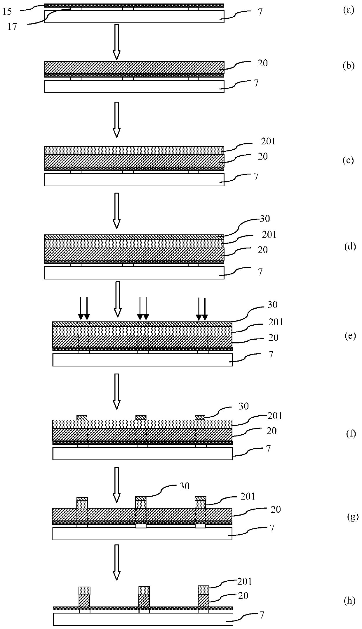
[0063] Implementation mode one, such as image 3 shown. This solution is preferably applicable to hydrophilic SOG materials with a baking temperature of ≤150° C., so as to reduce damage to the pixel wall 20 caused by baking. More preferably, it is suitable for hydrophilic SOG materials with a baking temperature of ≤120°C; even more preferably, it is suitable for hydrophilic SOG materials with a baking temperature of ≤100°C.
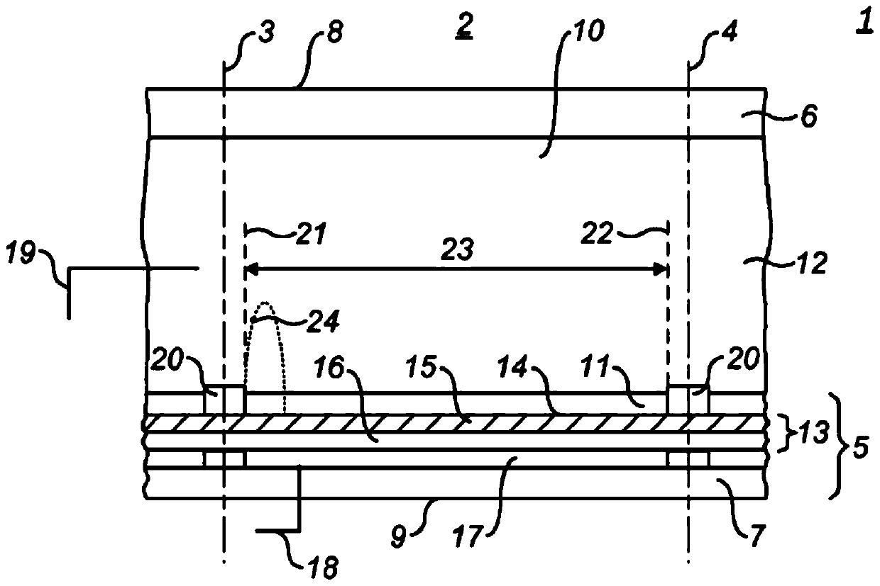
[0064] First, a substrate 7 is provided, an electrode 17 is arranged on the substrate 7, and a hydrophobic insulating layer 15 is arranged on the electrode; as image 3 (a). Of course, a dielectric layer 16 may also be provided between the electrode 17 and the hydrophobic insulating layer 15 .
[0065] The next step of manufacturing is to arrange the pixel wall 20 material layer on the surface of the hydrophobic insulating layer 15, such as image 3 (b). The material of the pixel wall 20 may be photoresist (for example, SU-8), which is pre-dried afte...
Embodiment approach 2
[0077] Implementation mode two, such as Figure 4 shown. This solution is preferably applicable to hydrophilic SOG materials with a baking temperature ≥ 120°C. Further preferably, it is suitable for a hydrophilic SOG material with a baking temperature ≥ 150°C.
[0078] First, a substrate 7 is provided, an electrode 17 is arranged on the substrate 7, and a hydrophobic insulating layer 15 is arranged on the electrode; as Figure 4(a). Of course, a dielectric layer 16 may also be provided between the electrode 17 and the hydrophobic insulating layer 15 .
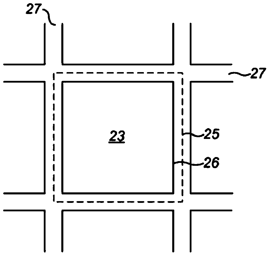
[0079] The next step of manufacture is to prepare the pixel wall 20 as Figure 4 (b)~4(c). The pixel wall 20 can be arranged on the surface of the hydrophobic insulating layer 15 in the first region 27 by a known method, and has a convex shape. A known method may include spin-coating a pixel wall material on the surface, the material may be photoresist (for example, SU-8), for photoresist pixel wall material, the pixel wa...
PUM
| Property | Measurement | Unit |
|---|---|---|
| thickness | aaaaa | aaaaa |
| thickness | aaaaa | aaaaa |
| thickness | aaaaa | aaaaa |
Abstract
Description
Claims
Application Information


