Ultrasonic imaging method and ultrasonic imaging device for realizing high-sensitivity imaging
An ultrasonic imaging method and high-sensitivity technology, applied in ultrasonic/sonic/infrasound equipment control, ultrasonic/sonic/infrasonic diagnosis, ultrasonic/sonic/infrasonic Permian technology, etc. Good or bad quality cannot be predicted in advance, etc., to achieve high imaging sensitivity, avoid exceeding the limit, and improve the effect of sensitivity
- Summary
- Abstract
- Description
- Claims
- Application Information
AI Technical Summary
Problems solved by technology
Method used
Image
Examples
Embodiment 1
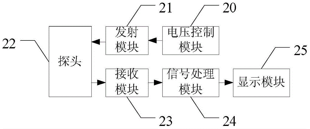
[0039] This embodiment provides an ultrasonic imaging device, such as figure 2 As shown, it includes: a voltage control module 20 , a transmitting module 21 , an ultrasonic probe 22 , a receiving module 23 , a signal processing module 24 and a display module 25 . The system controls the shape of the transmission pulse and the array elements involved in the transmission, respectively controls the transmission voltage of each imaging mode through the voltage control module 20, and the ultrasonic probe 22 converts the excited electrical signal into an acoustic signal, and transmits it to the object to be detected (for example, human tissue ). The ultrasonic echo reflected by the object to be detected is received by each element of the ultrasonic probe and converted into an electrical signal to form an ultrasonic echo signal (ultrasonic echo signal). The receiving module 23 receives these ultrasonic echo signals (ultrasonic echo signals) and performs corresponding processing, an...
Embodiment 2
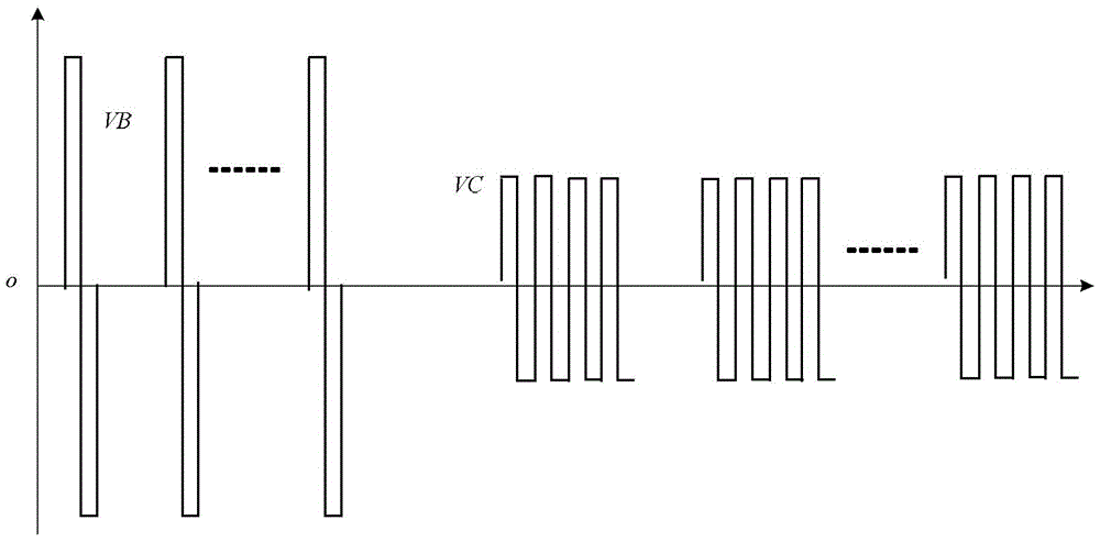
[0067] The difference between this embodiment and Embodiment 1 lies in the restriction on the increased second-mode pulse emission voltage (ie, the aforementioned second mode second voltage) in the high-sensitivity imaging step. At this time, the specific scanning process involved in the emission module or the emission step of this embodiment is as follows: Figure 6 As shown, under the normal imaging step, the working voltage of the second mode scan is relatively small. When the high-sensitivity imaging step is triggered, the emission voltage VC of the second mode scan is instantly increased to the maximum limit of MI stipulated by the FDA, which meets the requirements of medical ultrasound. The output index standard, and the emission voltage VB of the first mode scan is correspondingly reduced. After the high-sensitivity imaging step continues to work for the first preset time t1, it will automatically switch to the normal imaging step, and the normal imaging step will contin...
Embodiment 3
[0069] Based on Embodiment 1, in this embodiment, after switching from the high-sensitivity imaging step back to the normal imaging step, the normal imaging step continues to work for a period of time (such as the second preset time t2), and the second preset time is greater than or equal to the preset failure time. When implemented, t1 and t2 are limited to: after the ultrasonic imaging device switches back and forth between the high-sensitivity imaging step and the normal imaging step for several (t1+t2) hours, the surface temperature rise of the ultrasonic probe meets the requirements on the probe surface temperature rise in medical ultrasound. Restricted standards. Therefore, it can be ensured that the ultrasonic imaging device will not continue to work at higher emission energy, and finally ensure that the temperature rise of the probe surface will not exceed the requirements of IEC regulations during all working hours.
[0070] IEC stipulates that in any case, the tempe...
PUM
 Abstract
Description
Claims
Application Information


