Formation method of polysilicon gate
A polysilicon gate, polysilicon layer technology, applied in electrical components, semiconductor/solid-state device manufacturing, semiconductor devices, etc., can solve problems such as poor performance and impact of semiconductor devices, and achieve the advantages of reducing line width roughness and reducing manufacturing costs. Effect
- Summary
- Abstract
- Description
- Claims
- Application Information
AI Technical Summary
Problems solved by technology
Method used
Image

Examples
no. 2 example
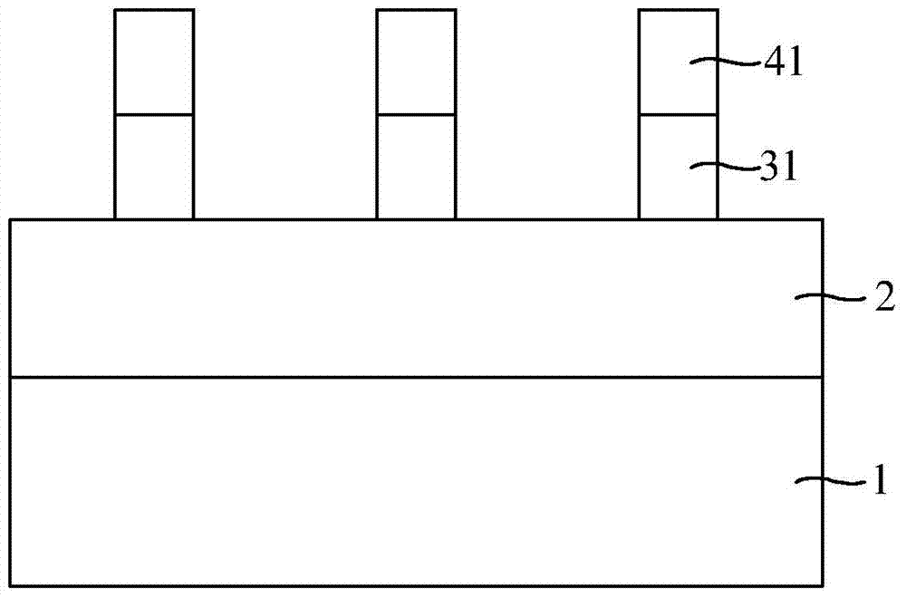
[0066] The difference between the second embodiment and the first embodiment is that in the second embodiment, the method for forming the patterned mask layer includes: forming a hard mask layer on the polysilicon layer, The bottom anti-reflection layer on the layer and the photoresist layer on the bottom anti-reflection layer; the photoresist layer and the bottom anti-reflection layer are patterned; the patterned photoresist layer is used as a mask to The hard mask layer is etched to form the patterned mask layer; the patterned photoresist layer and bottom anti-reflection layer are removed.
no. 3 example
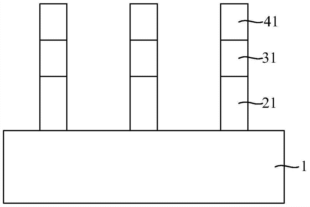
[0068] The difference between the third embodiment and the first embodiment is that in the third embodiment, the method for forming the patterned mask layer includes: forming a bottom anti-reflection layer on the polysilicon layer, and A photoresist layer on the reflection layer; patterning the photoresist layer and the bottom anti-reflection layer to form the patterned mask layer.
no. 4 example
[0070] The difference between the fourth embodiment and any of the first to third embodiments is that in the fourth embodiment, after the second anisotropic dry etching and before the third anisotropic dry etching , further comprising: removing the patterned mask layer.
[0071] In the above-mentioned first to third embodiments, after the third anisotropic dry etching, the patterned mask layer formed above the polysilicon gate has other uses in the subsequent process, so in the second anisotropic After the dry etching and before the third anisotropic dry etching, the patterned mask layer is not removed.
[0072] In the present invention, in the second anisotropic dry etching step, the temperature of the heating condition is not limited to the given embodiment, as long as the temperature is higher than room temperature.
PUM
 Abstract
Description
Claims
Application Information