Pattern transfer method

A graphics transfer and graphics technology, applied in the direction of electrical components, semiconductor/solid-state device manufacturing, circuits, etc., can solve problems such as low hardness, affecting device performance, and being vulnerable to damage, achieving high ion implantation efficiency and reducing line width roughness Degree, the effect of reducing equipment cost

Active Publication Date: 2017-04-19
BEIJING NAURA MICROELECTRONICS EQUIP CO LTD
View PDF7 Cites 0 Cited by
  • Summary
  • Abstract
  • Description
  • Claims
  • Application Information

AI Technical Summary

Problems solved by technology

[0005] First, the substrate needs to be transferred from the etching chamber to the deposition chamber to form an amorphous carbon layer, and then transferred from the deposition equipment to the etching chamber to continue the etching process. The etching process also needs to increase the etching process. The step of etching the amorphous carbon, therefore, not only causes complex process, long process time, low yield; but also increases the equipment cost of the deposition chamber, and the economic benefit is low
[0006] Second, because the amorphous carbon structure is loose and porous, and its hardness is relatively low, it is easily damaged in the etching process, resulting in high line width roughness, which may affect device performance.

Method used


Image

  • Pattern transfer method
  • Pattern transfer method
  • Pattern transfer method

Examples


Embodiment Construction

[0023] In order to enable those skilled in the art to better understand the technical solution of the present invention, the graphic transfer method provided by the present invention will be described in detail below in conjunction with the accompanying drawings.

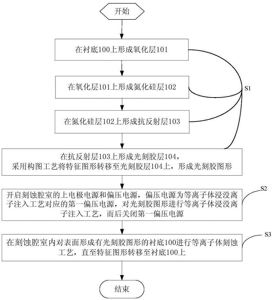
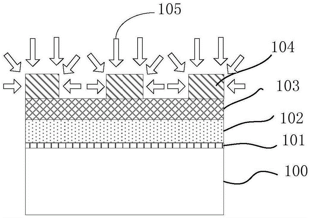
[0024] figure 1 A flow chart of a graphics transfer method provided by an embodiment of the present invention; figure 2 for figure 1 A schematic diagram of step S2 is shown. Please also refer to figure 1 and figure 2 , the pattern transfer method provided by the embodiment of the present invention is used to transfer a characteristic pattern onto the substrate 100, and the so-called characteristic pattern refers to a pattern designed to prepare a semiconductor device. Specifically, the graph transfer method includes the following steps:

[0025] In step S1 , a photoresist layer 104 is formed on the substrate 100 , and a patterning process is used to transfer the characteristic pattern onto the photoresist lay...


PUM


Abstract

The invention provides a pattern transfer method, which is used for transferring a characteristic pattern to a substrate. The method comprises the following steps: S1) forming a photoresist layer on the substrate, and transferring the characteristic pattern to the photoresist layer through the composition technology to form a photoresist pattern; S2) turning on an excitation power supply and a grid bias power supply in an etching chamber, wherein the grid bias power supply is a first grid bias power supply corresponding to plasma immersion ion implantation technology, carrying out plasma immersion ion implantation on the photoresist pattern, and then, turning off the first grid bias power supply; and S3) carrying out plasma etching on the substrate, on the surface of which the photoresist pattern is formed, in the etching chamber until the characteristic pattern is transferred to the substrate. The pattern transfer method can reduce line width roughness of each line of the photoresist pattern in situ, so that process is simplified to a great extent, process time is reduced and device cost is reduced; and besides, line width roughness of each line of the photoresist pattern can be further reduced, thereby facilitating accurately transferring the pattern to the substrate.

Description

technical field [0001] The invention belongs to the field of semiconductor device manufacturing, and in particular relates to a pattern transfer method. Background technique [0002] In the field of semiconductor device manufacturing, in order to reduce the manufacturing cost of devices, it is necessary to prepare as many devices as possible on a substrate with a certain area, which requires the feature size of the device to be as small as possible. At present, the lithography process determines the minimum feature size of the device. In order to accurately transfer the feature pattern with a smaller feature size to the substrate, the lithography process needs to face the challenge of reducing the line width roughness (LWR) as much as possible. The so-called line width roughness refers to the deviation of the device line relative to the ideal device line. Specifically, the shape of the ideal device line is generally a straight line, but in fact the shape of the device line i...

Claims


Application Information

Patent Timeline
Patent Type & Authority Applications(China)
IPC IPC(8): H01L21/027
CPCH01L21/0273H01L21/0274
Inventor 罗巍
Owner BEIJING NAURA MICROELECTRONICS EQUIP CO LTD
Why Eureka
Try Eureka