Formation method of semiconductor structure

A semiconductor and graphics technology, applied in the direction of semiconductor devices, etc., can solve the problem that the electrical performance of the semiconductor structure needs to be improved, and achieve the effect of avoiding channel length changes, good consistency, and small line width roughness.

Active Publication Date: 2018-02-16
SEMICON MFG INT (SHANGHAI) CORP
View PDF5 Cites 0 Cited by
  • Summary
  • Abstract
  • Description
  • Claims
  • Application Information

AI Technical Summary

Problems solved by technology

[0004] However, the electrical performance of the semiconductor structures formed by the prior art needs to be improved

Method used


Image

  • Formation method of semiconductor structure
  • Formation method of semiconductor structure
  • Formation method of semiconductor structure

Examples


Embodiment Construction

[0032] It can be seen from the background art that the electrical performance of the semiconductor structure formed in the prior art needs to be improved.

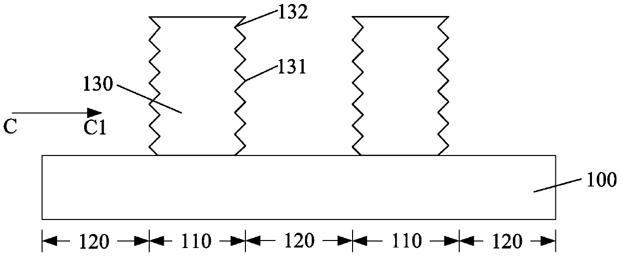
[0033] Such as figure 2 as shown, figure 2 A cross-sectional schematic diagram of a semiconductor structure formed by a method provided in the prior art, including: a substrate 100, the substrate 100 including a gate region 110 and a doped region 120 adjacent to the gate region 110, the gate region 110 includes an active region and an isolation region adjacent to the active region, and the width dimension of the gate region 110 (that is, the distance from the source region to the drain region), the width dimension of the active region and the isolation region are consistent, and the formed gate The pole 130 covers the active area and part of the isolation area. Ideally, the width dimension of the patterned photoresist layer is consistent with the width dimension of the active region, so that the length of the formed ch...


PUM


Abstract

A formation method of a semiconductor structure is disclosed. The method comprises the following steps of providing a surface possessing a grid film substrate, wherein a grid pattern film including a hard mask layer material layer and a silicon material layer covers a grid film surface; forming a pattern layer on a grid pattern film surface; taking the pattern layer as a mask layer and etching a part of the grid pattern film to form a grid pattern layer, wherein the grid pattern layer comprises a hard mask layer and a silicon layer located on a hard mask layer surface; and a sidewall surface of the silicon layer, which is vertical to a first direction, possesses first line width roughness; carrying out repairing etching processing on the silicon layer sidewall vertical to the first direction so that the silicon layer sidewall surface possesses second line width roughness less than the first line width roughness; taking the grid pattern layer as the mask layer to etch a grid film and forming a grid on a substrate surface; and forming a source area and a leakage area in the substrate of two sides of a grid sidewall vertical to the first direction. By using the method, the line width roughness of the grid pattern layer is reduced so that formed grid quality is increased and electric performance of the semiconductor structure is optimized.

Description

technical field [0001] The invention relates to the technology in the field of semiconductor manufacturing, in particular to a method for forming a semiconductor structure. Background technique [0002] At present, with the rapid development of semiconductor manufacturing technology, semiconductor devices are developing towards higher component density and higher integration in order to achieve faster computing speed, larger data storage capacity and more functions. The corresponding semiconductor process has higher and higher requirements for etching, and the etching of the gate is particularly critical. The etching quality of the gate not only determines the gate size of the semiconductor device, but also determines the saturation drain current of the semiconductor device. and other electrical parameters. [0003] The formation process of semiconductor device in the prior art comprises the following steps, with reference to figure 1 , step S11, providing a substrate, the...

Claims


Application Information

Patent Timeline
Patent Type & Authority Patents(China)
IPC IPC(8): H01L21/28
Inventor 张海洋张璇
Owner SEMICON MFG INT (SHANGHAI) CORP
Why Eureka
Try Eureka