Method of fabricating SOI wafer

a technology of soi wafers and soi layers, which is applied in the direction of basic electric elements, electrical apparatus, semiconductor devices, etc., can solve the problems of increasing the risk of affecting the above-described method suffers from the drawbacks described, and the thickness distribution of the polished soi layer is more likely to worsen. , to achieve the effect of reducing the roughness of the separation surfa

Inactive Publication Date: 2008-01-22
SHIN-ETSU HANDOTAI CO LTD
View PDF8 Cites 14 Cited by
  • Summary
  • Abstract
  • Description
  • Claims
  • Application Information

AI Technical Summary

Benefits of technology

[0016]The present inventors experimentally re-verified ion implantation dose possibly causing the separation of the bond wafer in the Smart-Cut process, and obtained new findings which have never known before. It is necessary to adjust ion implantation energy in order to adjust the depth of formation of the separatory ion implanted layer depending on a desired thickness of the SOI layer. The critical ion dose causative of the separation has conventionally been believed as constant irrespective of ion implantation depth, but it was revealed from the investigations by the present inventors that a smaller ion implantation depth can cause the separation under a lower dose. In other words, the smaller the depth of formation of the separatory ion implanted layer becomes, the smaller the critical dose necessary for the separation becomes. On the other hand, roughness of the separation surface is also related to the ion implantation dose, wherein a smaller dose results in a smaller roughness of the separation surface. The ion implantation dose is therefore set to a small value for the case where the depth of formation of the separatory ion implanted layer measured from the first main surface is small. A small dose can reduce the roughness of the separation surface, and can improve uniformity in the thickness of the SOI layer even when it is formed to a small thickness.
[0017]The planarization step can further improve uniformity in the thickness of the SOI layer if the step further comprises a step of polishing the separation surface side of the bonded silicon single crystal film. More specifically, a smaller roughness of the separation surface of the bonded silicon single crystal film obtained by the separation makes it possible to set a smaller value for the polishing stock removal of the separation surface of the bonded silicon single crystal film in the polishing step. In other words, reduction in the roughness of the separation surface can reduce the polishing stock removal of the separation surface of the bonded silicon single crystal film in the polishing step, and can effectively reduce influences of the intra-wafer non-uniformity of the polishing stock removal.
[0018]In an exemplary case where the thickness of the SOI layer to be obtained is small while assuming the thickness of the insulating film formed on the bond wafer as constant, the ion implantation dose is set small corresponding to the small thickness, and also the polishing stock removal of the separation surface of the bonded silicon single crystal film in the polishing step is set small. In other words, a smaller thickness of the bonded silicon single crystal film, and consequently of the final SOI layer, results in a shallower position of formation of the separatory ion implanted layer, reduces the ion implantation dose, reduces the polishing stock removal in the planarization of the separation surface, and reduces influences of the non-uniformity in the polishing stock removal to a considerable degree. This makes it possible to suppress variations in the intra-wafer and inter-wafer uniformity of the thickness of the SOI layer to a sufficiently low level, despite the thickness of the SOI layer is extremely small.

Problems solved by technology

The above-described method, however, suffers from the drawbacks described in the next.
This method may be successful in removing roughness component with a short wavelength on the separation surface in a relatively easy manner, but is disadvantageous in that another intra-wafer non-uniformity in the polishing stock removal is newly added.
In particular for the case where the surface roughness of the separation surface is large, the thickness distribution of the polished SOI layer becomes more likely to worsen because the polishing stock removal becomes larger.
This sort of non-uniformity in the thickness is inevitable in the light of current technical level of mirror polishing, and may not specifically raise a serious problem so far as the thickness of the SOI layer remains at a level of approximately 100 nm or more.
In this case, the above-described level of non-uniformity in the thickness reaches ten to several tens of percent of a target average thickness, so that it is apparent that the non-uniformity directly results in quality variation of the semiconductor devices using the SOI wafer, and in lowered production yield.

Method used


Image

  • Method of fabricating SOI wafer
  • Method of fabricating SOI wafer
  • Method of fabricating SOI wafer

Examples


Embodiment Construction

[0027]The following paragraphs will describe best modes for carrying out the invention.

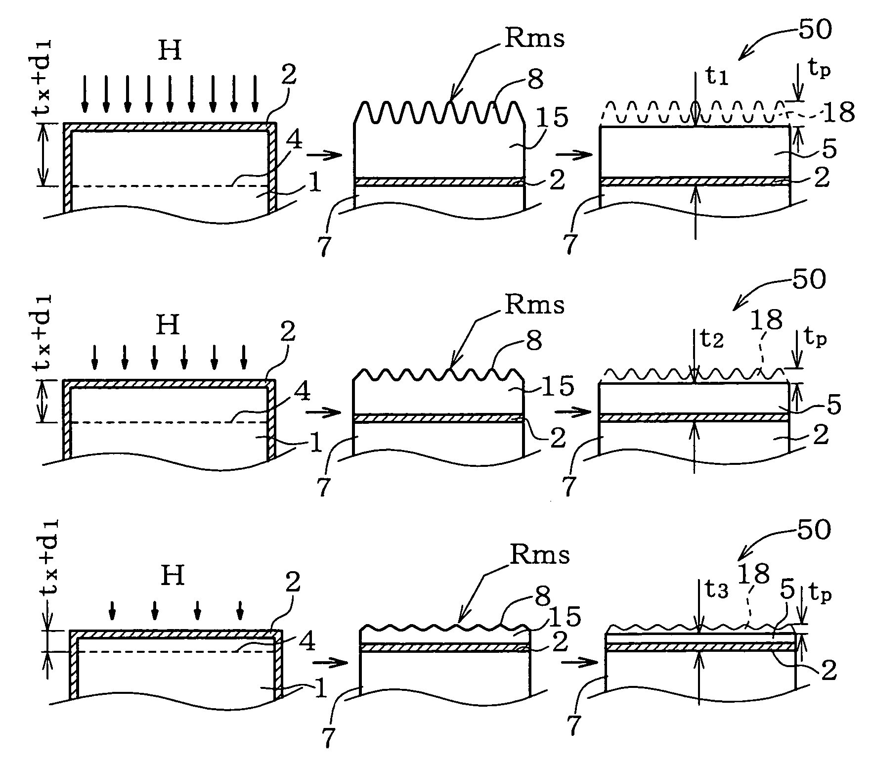
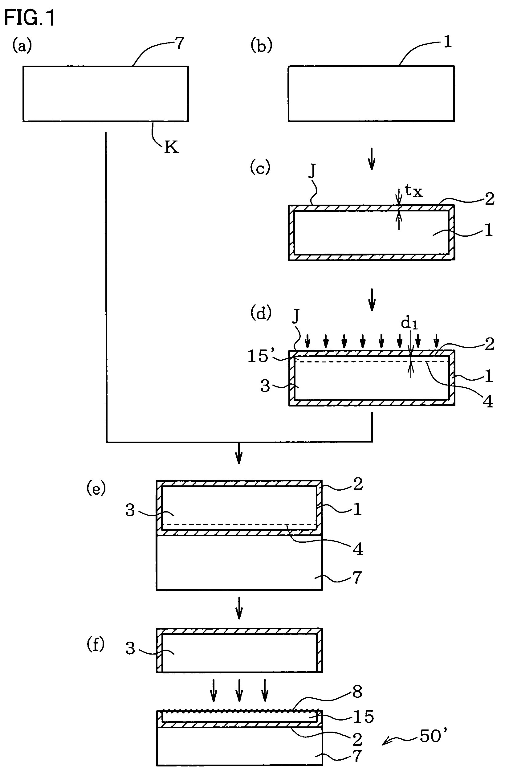
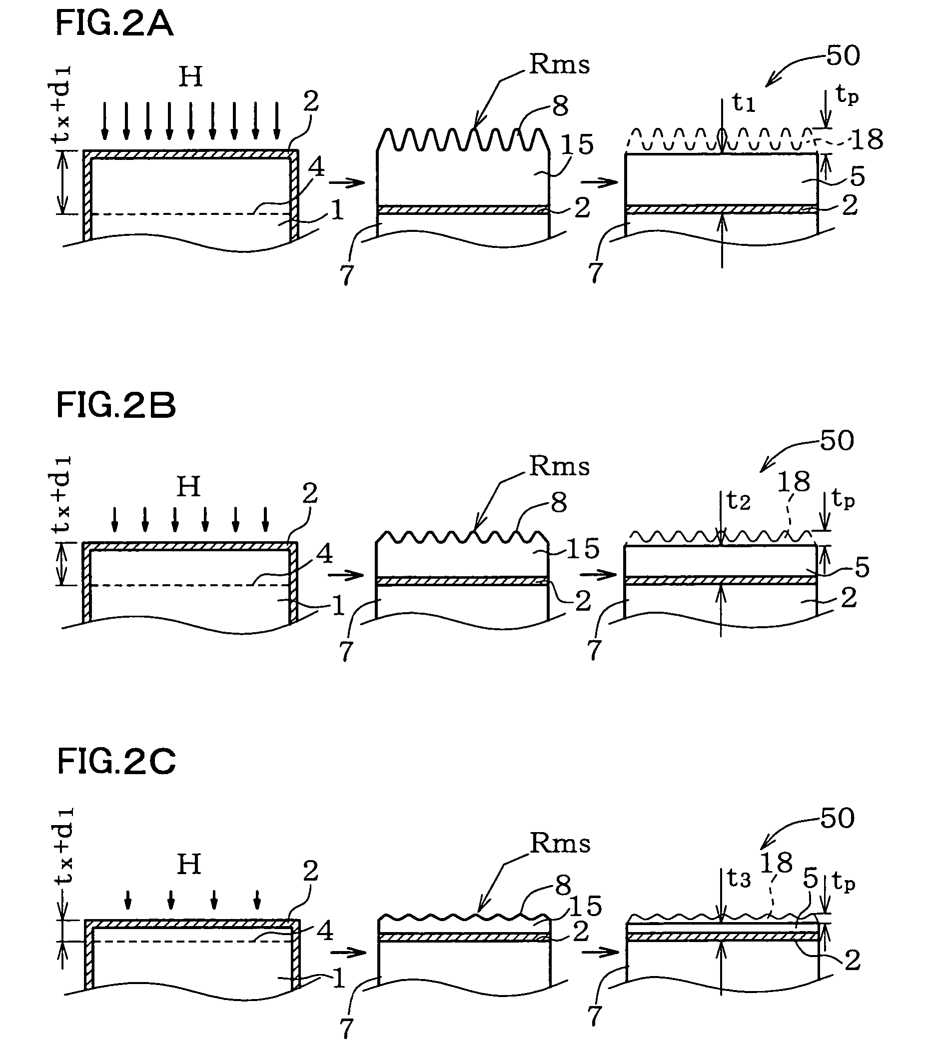
[0028]FIG. 1 is a drawing explaining a basic embodiment of the method of fabricating an SOI wafer according to the present invention. First, a base wafer 7 shown in step (a) as a first substrate typically composed of silicon single crystal, and a bond wafer 1 shown in step (b) as a second silicon single crystal substrate are obtained. The bond wafer 1 has, as shown in step (c), a silicon oxide film 2 as an insulating film formed at least on a first main surface J side thereof. The silicon oxide film 2 can be formed by thermal oxidation such as wet oxidation or dry oxidation, and it is also allowable to adopt a method such as CVD (chemical vapor deposition). Thickness of the silicon oxide film tx is adjusted to approximately 50 nm to 2 μm, both ends inclusive, considering that it is used as an insulating layer typically for MOS-FET. The base wafer 7 may be an insulating substrate such as quartz sub...


PUM


Abstract

In order to adjust thickness of a bonded silicon single crystal film 15 depending of thickness of an SOI layer 5 to be obtained, depth of formation d1+tx of a separatory ion implanted layer 4, measured from a first main surface J, in the separatory ion implanted layer formation step is adjusted through energy of the ion implantation. Dose of the ion implantation is set smaller as the depth of formation measured from the first main surface J becomes smaller. A smaller dose results in a smaller surface roughness of the separation surface, and makes it possible to reduce polishing stock removal of the separation surface of the bonded silicon single crystal film in the planarization step. Uniformity in the thickness of the SOI layer can consequently be improved even for the case where a thin SOI layer has to be formed. The present invention is therefore successful in providing a method of fabricating an SOI wafer capable of suppressing variations in the intra-wafer and inter-wafer uniformity of the thickness of the SOI layer to a sufficiently low level, even for the case where a required level of the thickness of the SOI layer is extremely small.

Description

FIELD OF THE INVENTION[0001]The present invention relates to a method of fabricating an SOI wafer.BACKGROUND ART[0002]In the field of mobile communication using mobile phones or the like, it is becoming general to handle high frequency signals of several hundreds of megahertz, and this raises needs for semiconductor devices excellent in high-frequency characteristics. For example, semiconductor devices such as CMOS-IC and high-voltage-resistant-type IC adopt a so-called SOI wafer which is configured by forming a silicon oxide insulating layer (buried oxide film) on a silicon single crystal substrate (also referred to as “base wafer”, hereinafter), and by stacking thereon another silicon single crystal layer as an SOI (silicon on insulator) layer. For the case where the SOI wafer is applied to semiconductor devices for high-frequency use, it is necessary to use a silicon single crystal having a large resistivity as the base wafer, in view of suppressing high-frequency loss.[0003]Bond...

Claims


Application Information

Patent Timeline
Patent Type & Authority Patents(United States)
IPC IPC(8): H01L21/30H01L21/46H01L21/02H01L21/265H01L21/762H01L27/12
CPCH01L21/265H01L21/26506H01L21/76224H01L21/76254H01L21/20H01L27/12
Inventor AGA, HIROJIMITANI, KIYOSHI
Owner SHIN-ETSU HANDOTAI CO LTD
Why Eureka
Try Eureka