[0023] Now will refer to the attached drawings by example image 3 with Figure 5 To describe the preferred form of the present invention.
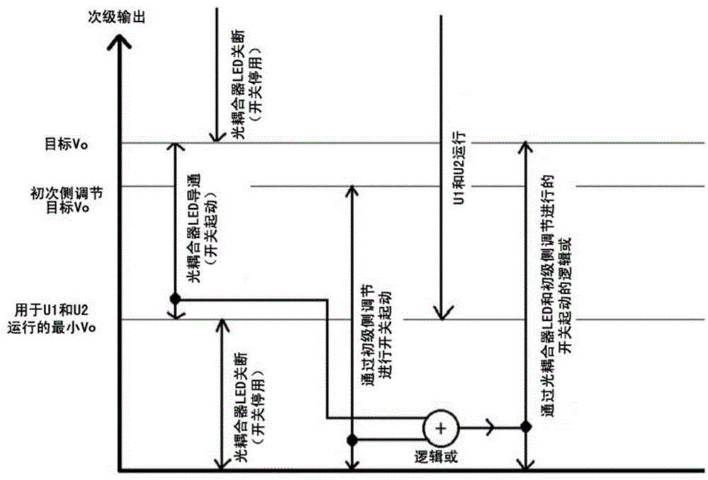
[0024] Reference image 3 with Figure 4 , Which shows that the optocoupler feedback control is added to the primary side regulation switching converter circuit as follows, where image 3 , The primary adjustment target Vo should be equal to or greater than the target Vo.
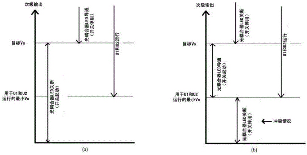
[0025] The conduction of the optocoupler LED can start the switching operation. In other words, it can be regarded as adding the primary side regulation control to the switching converter circuit with optocoupler feedback, so that the switching operation can be started when the LED of the optocoupler is turned on. In either case, the switching operation is a probable logic start.
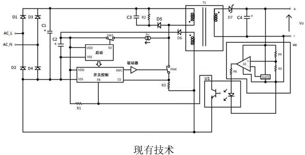
[0026] in Figure 4 Among them, T1 is a transformer required for switching with PSW as a power switching device. Diodes D1, D2, D3, and D4 form a bridge rectifier circuit that converts AC input into pulsating DC, and capacitor C1 filters the pulsating DC into high-voltage DC, which is used as a power source for the primary winding of transformer T1 enter.
[0027] During the start-up, the switch SW1 is closed and the start-up current source Isu charges the VDD decoupling capacitor C2 to the level at which the switching starts. Then SW1 is turned off and the switching operation will continue until the output voltage at the secondary side reaches the target level for the first time. Then the switching will be activated or deactivated according to the secondary output voltage to maintain the secondary voltage at the target value.
[0028] The activation part on the primary side controls the activation sequence, and the switch control device (IC) handles the switching operation.
[0029] When the switching is started, the switching control device (IC) generates an output signal SWC with a correct duty ratio, and the output signal SWC is used as the input of the driver (DRV) of the main switching device PSW. The primary-side switching current can be measured by monitoring the voltage at the resistor R3 using the CS node. When the PSW is turned on, the primary inductance of the transformer T1 stores energy. When the PSW is turned off, the stored energy is transferred to the secondary side and auxiliary side of the transformer T1. On the secondary side, diode D7 rectifies the signal from the secondary winding of transformer T1. Capacitor C4 is the output filter. The output detector circuit U2 monitors the output voltage Vo. When Vo is lower than the target value, the comparator A1 turns on the LED of the optocoupler U1 to instruct the primary circuit to deliver more power. When Vo is higher than the target value, the comparator A1 will turn off the LED of the photocoupler U1 to notify the primary circuit to stop the switching operation. In this way, the output voltage is adjusted to its target value. During each switching cycle, the auxiliary winding of the transformer T1 also provides energy to charge the VDD decoupling capacitor C2 via the diode D6.
[0030] The diode D5, the resistor R2 and the capacitor C3 form a snubber circuit to absorb transient energy, so as to reduce transient oscillations during switching.
[0031] Resistors R7 and R8 together with the primary side regulating voltage sensing circuit U3 monitor the output voltage by monitoring the voltage at the auxiliary winding when energy is transferred to the secondary side during each switching cycle. When the secondary side output voltage is lower than the target, the output of the comparator A2 will be high, and the switching operation will be started.
[0032] Alternatively, the primary side regulation sensing can be performed directly at the VDD node.
[0033] The logic OR gate G1 combines the “enable” signal from the primary side regulation and the feedback signal from the optocoupler, so that whenever the secondary voltage is lower than the target, or even the most extreme, the output voltage is lower than the output detector circuit U2 and the light At the minimum operating voltage of the coupler LED, the switching operation can be started.
[0034] At the secondary side voltage detection and LED driver circuit (U2), and figure 1 Compared with the situation in the middle, the input of the comparator A1 is swapped. This means that the LED of the optocoupler is only turned on figure 1 The logic in the situation is reversed. Figure 4 U2 in can be integrated into a three-terminal device.
[0035] The secondary output voltage is basically determined by the secondary side voltage detection and LED driver circuit with excellent dynamic load response. Hysteresis can be added to the voltage detection circuit. This will increase the output ripple voltage and further reduce the standby power.
[0036] Modifications can be made to the secondary side voltage detection and LED driver circuit to incorporate the output current detection function, turning the device into an output voltage and current detection device. Figure 5 It is the block diagram together with the transformer secondary circuit. in Figure 5 In, the resistor R1 converts the output current into a voltage, which is monitored by a current detector. A3 is a "differential-to-single-ended" amplifier with a suitable gain factor, matching the current limit with the reference voltage Vref. Comparator A2 compares the measured output current with its limit. The resistors R2 and R3 and the comparator A1 together Figure 4 The same way as in plays the role of monitoring the output voltage. The LED of the optocoupler U1 at the secondary circuit turns on when the output voltage and output current are lower than the target. This voltage and current detection circuit can be integrated into a four-terminal device (U2). by using Figure 4 The device with the above-mentioned primary side circuit can realize CV/CC switch conversion.