Display panel, display panel manufacturing method and display

A technology for display panels and array substrates, applied in the directions of instruments, nonlinear optics, optics, etc., can solve the problems of broken metal data lines 13 and increased defect rate of products, and reduce the number of metal grids, reduce defect rate, reduce Effect of Fracture Chance

Active Publication Date: 2015-03-25
SHENZHEN CHINA STAR OPTOELECTRONICS TECH CO LTD
View PDF8 Cites 11 Cited by
  • Summary
  • Abstract
  • Description
  • Claims
  • Application Information

AI Technical Summary

Problems solved by technology

[0006] However, in the case of a narrow connection area of ​​the COF module 1S, the width of the data line 13 in the area of ​​the digital sign 2 is too small, which can easily cause the metal data line 13 to break and form a vertical thin line, resulting in an increase in the defective rate of the product

Method used


Image

  • Display panel, display panel manufacturing method and display
  • Display panel, display panel manufacturing method and display
  • Display panel, display panel manufacturing method and display

Examples


Embodiment Construction

[0026] In order to make the object, technical solution and advantages of the present invention more clear, the present invention will be further described in detail below in conjunction with the accompanying drawings and embodiments. It should be understood that the specific embodiments described here are only used to explain the present invention, not to limit the present invention.

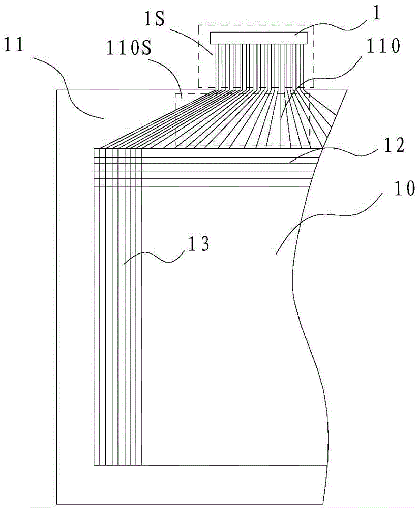
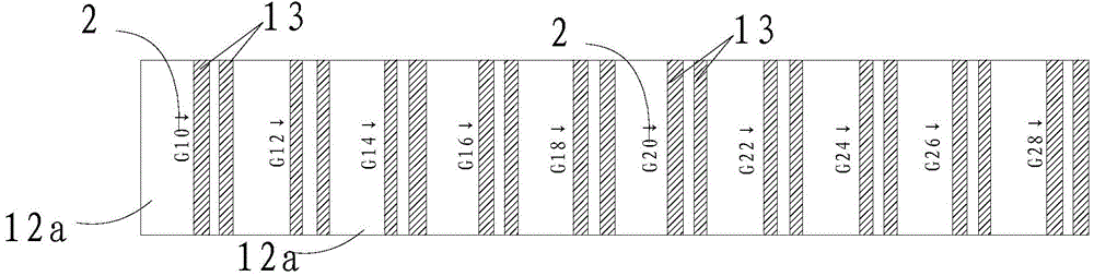
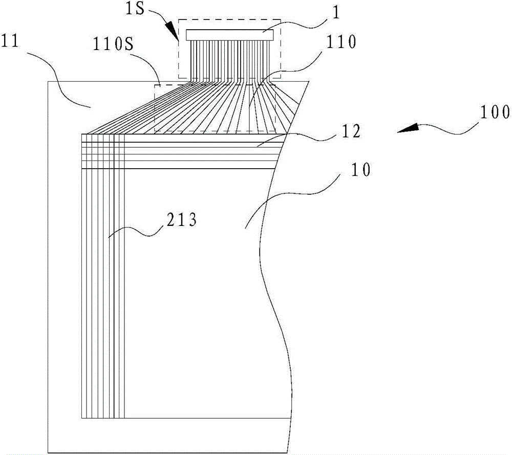
[0027] like image 3 As shown, the display panel 100 of the embodiment of the present invention includes an active area 10 and a peripheral circuit area 11. The active area 10 has pixel units and is provided with a plurality of parallel and spaced data lines 213; the peripheral circuit area 11 does not have pixels unit, and is provided with a fan-out lead 110 for connecting the driver chip 1 . combine Figure 4 , wherein, the TFT array substrate (not shown) includes a glass substrate 212S, a gate 212a, two insulating layers 212d, a transparent conductive film (ie ITO) layer 212b and a source e...


PUM


Abstract

The invention discloses a display panel. The display panel comprises an active region with pixels and a peripheral circuit region without pixels. A plurality of parallel data lines at intervals are arranged in the active region; fan-out leads used for connection with a driver chip are arranged in the peripheral circuit region; the active region is provided with first identifications, and the first identifications are formed at intervals on a plurality of ITO (indium tin oxide) layers of a thin film transistor array substrate by etching and used for distinguishing the data lines connected with the fan-out leads. By the first identifications arranged on the at least one ITO layer of the thin film transistor array substrate of the display panel, directly etching number identifications on metal grids in the prior art is replaced, quantity of the metal grids with etched number identifications is greatly decreased, each single metal data line on the display panel can be wider, and accordingly possibility of breakage of the metal data lines is reduced while ratio of rejects due to vertical lines generated on products is decreased. The invention further provides a display.

Description

technical field [0001] The invention relates to the technical field of liquid crystal display, in particular to a display panel, a manufacturing method of the display panel and a display. Background technique [0002] The liquid crystal display panel is composed of a color filter substrate with a color filter layer, a thin film transistor (TFT) array substrate and a liquid crystal layer arranged between the two substrates. [0003] The current liquid crystal display panel is mainly based on the development trend of thin and light large screen, which requires a new generation of packaging technology with high density, small volume and free installation to meet the above requirements. Based on this, COF (Chip on Film, ie Chip-on-film) packaging technology emerged as the times require. This technology uses a flexible circuit board as a packaged chip carrier to bond the chip with the flexible substrate circuit. It is a grain soft film construction technology that fixes the drive...

Claims


Application Information

Patent Timeline
Patent Type & Authority Applications(China)
IPC IPC(8): G02F1/1362G02F1/1368G02F1/1333
CPCG02F1/136286G02F1/1368G02F1/133374
Inventor 郑娜
Owner SHENZHEN CHINA STAR OPTOELECTRONICS TECH CO LTD
Why Eureka
Try Eureka