Method for forming semiconductor device

A semiconductor and device technology, applied in the field of semiconductor device formation, can solve the problems of poor reliability of isolation structure, breakdown or leakage of semiconductor devices, etc., and achieve the effect of improving reliability, stability and corrosion resistance

Active Publication Date: 2015-03-25
SEMICON MFG INT (SHANGHAI) CORP
View PDF4 Cites 5 Cited by
  • Summary
  • Abstract
  • Description
  • Claims
  • Application Information

AI Technical Summary

Problems solved by technology

[0005] The introduction of embedded silicon germanium technology and embedded carbon silicon technology can improve the carrier mobility of semiconductor devices, but in practical applications, it is found that the carrier mobility of semiconductor devices has been improved, but the reliability of the isolation structure of semiconductor devices Poor performance, semiconductor devices are prone to breakdown or leakage

Method used


Image

  • Method for forming semiconductor device
  • Method for forming semiconductor device
  • Method for forming semiconductor device

Examples


Embodiment Construction

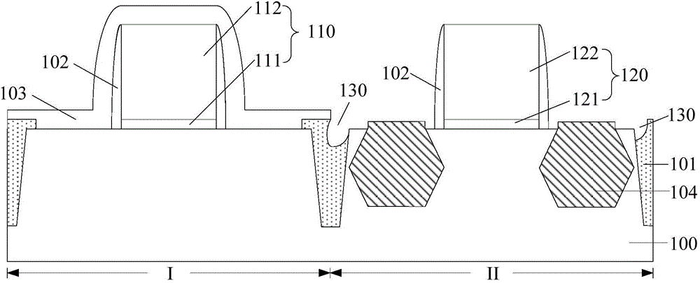
[0035] As mentioned in the background art, there are problems that need to be solved urgently in the semiconductor devices formed in the prior art. For example, in the process of manufacturing semiconductor devices, the isolation structure is excessively eroded, which leads to the deterioration of the ability of the isolation structure to isolate adjacent device regions, thereby affecting the semiconductor device. Device electrical performance and reliability.

[0036] To this end, the formation of semiconductor devices is studied. The formation method of semiconductor devices includes the following steps. Please refer to figure 1 , figure 1 A schematic diagram of a cross-sectional structure of a semiconductor device:

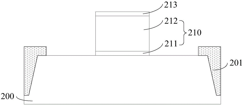
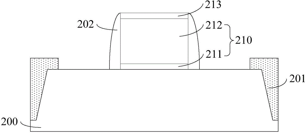
[0037] A semiconductor substrate 100 is provided, the semiconductor substrate 100 includes a first region I and a second region II, and the first region I and the second region II are separated by an isolation structure 101, the semiconductor substrate of the ...


PUM


Abstract

A method for forming a semiconductor device comprises the following steps: providing a semiconductor substrate, wherein the semiconductor substrate is internally provided with isolation structures, and the surface of the semiconductor substrate is provided with gate structures arranged between adjacent isolation structures; stably doping the isolation structures to enhance the corrosion resistance of the isolation structures; forming grooves in the semiconductor substrate at the two sides of each gate structure; cleaning the grooves after doping the isolation structures; and forming a stress layer filling the grooves. The stability of the isolation structures is increased, the anti-etching ability of the isolation structure material is improved, the situation in which the isolation structures are etched by a semiconductor device fabrication process is avoided, the reliability of the isolation structures is improved, the reliability of semiconductor devices is improved, the occurrence of breakdown or leakage is avoided, and the electrical performance of semiconductor devices is optimized.

Description

technical field [0001] The invention relates to the field of semiconductor manufacturing, in particular to a method for forming a semiconductor device. Background technique [0002] With the continuous development of semiconductor technology, carrier mobility enhancement technology has been widely studied and applied. Improving the carrier mobility in the channel region can increase the driving current of semiconductor devices and improve the performance of devices. [0003] In the existing manufacturing process of semiconductor devices, since stress can change the energy gap and carrier mobility of silicon materials, it has become more and more common means to improve the performance of semiconductor devices through stress. Specifically, by properly controlling the stress, the mobility of carriers (electrons in NMOS devices, holes in PMOS devices) can be increased, thereby increasing the driving current, thereby greatly improving the performance of semiconductor devices. ...

Claims


Application Information

Patent Timeline
Patent Type & Authority Applications(China)
IPC IPC(8): H01L21/762
CPCH01L21/76237H01L21/823481H01L21/823878
Inventor 何永根
Owner SEMICON MFG INT (SHANGHAI) CORP
Why Eureka
Try Eureka