
Circuit board processing method

A processing method and technology for circuit boards, which are applied in printed circuits, printed circuit manufacturing, and chemical/electrolytic methods to remove conductive materials, etc., can solve the problem that it is difficult to process high-precision and fine lines from thick copper circuit boards, and achieve good results. Etching, improving etching accuracy, inhibiting side etching effect

Inactive Publication Date: 2015-03-25
SHENNAN CIRCUITS
View PDF2 Cites 2 Cited by
  • Summary
  • Abstract
  • Description
  • Claims
  • Application Information

AI Technical Summary

Problems solved by technology

[0004] The embodiment of the present invention provides a circuit board processing method to solve the technical problem that it is difficult to process high-precision fine lines for thick copper circuit boards using the existing technology

Method used


Image

  • Circuit board processing method
  • Circuit board processing method
  • Circuit board processing method

Examples


Embodiment Construction

[0013] The embodiment of the present invention provides a method for processing a circuit board, which can solve the technical problem that it is difficult to process high-precision and fine lines for thick copper circuit boards using the prior art. A detailed description will be given below in conjunction with the accompanying drawings.

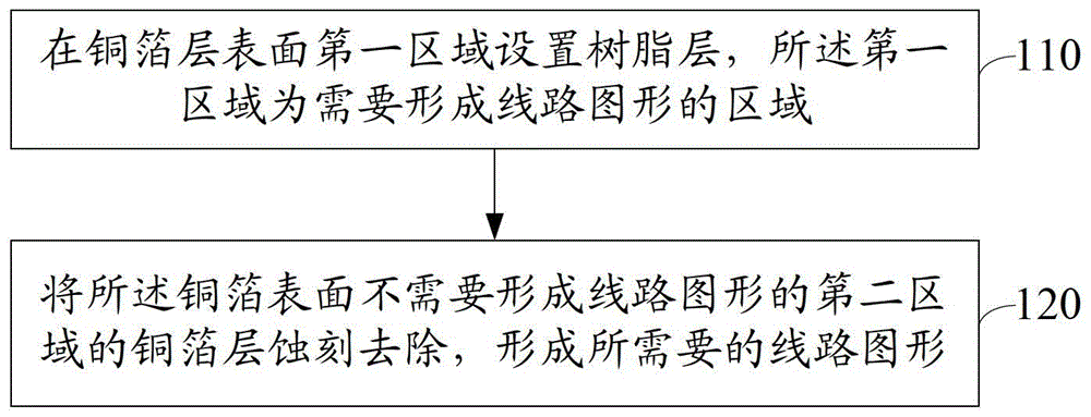
[0014] Please refer to figure 1 , the embodiment of the present invention provides a circuit board processing method, comprising:

[0015] 110. Arrange a resin layer on a first area on the surface of the copper foil layer, and the first area is an area where circuit patterns need to be formed.

[0016] In the embodiment of the present invention, resin is used instead of dry film as the anti-corrosion protection layer, which is mainly suitable for thick copper circuit boards with a copper thickness greater than or equal to 3 OZ, so as to improve the etching accuracy for thick copper circuit boards.

[0017] In one embodiment, before step 11...


PUM


Abstract

The invention discloses a circuit board processing method which includes the steps that a resin layer is arranged in a first area of the surface of a copper foil layer, and the first area is the area where a circuit graph needs to be formed; the part, in a second area where a circuit graph does not need to be formed, of the copper foil layer on the surface of copper foil is etched and removed, and a needed circuit graph is formed. According to the technical scheme, the resin layer is used for conducting anti-corrosion protection, due to the fact that the binding force of the resin layer and the copper foil layer is far larger than the binding force of a dry film and the copper foil layer, lateral etching of the resin layer can be better inhibited compared with that of the dry film, and therefore the etching precision can be improved, and a higher-precision fine circuit is manufactured.

Description

technical field [0001] The invention relates to the technical field of circuit boards, in particular to a circuit board processing method. Background technique [0002] In the existing circuit board processing technology, a dry film is usually used as an anti-corrosion protective layer on the surface of the copper foil layer, and then the area not protected by the dry film is etched to process the copper foil layer into a circuit pattern. [0003] Due to the influence of side erosion, for thick copper circuit boards with a copper foil layer thickness of not less than 3OZ (ounces, thickness unit, agreed to be 0.035mm), the density of circuit patterns processed by the above process is relatively sparse and the accuracy is poor, so it is difficult to process Produce high-precision fine lines. Contents of the invention [0004] An embodiment of the present invention provides a method for processing a circuit board to solve the technical problem that it is difficult to process...

Claims


Application Information

Patent Timeline
Patent Type & Authority Applications(China)
IPC IPC(8): H05K3/06
CPCH05K3/06H05K3/282H05K2203/0591
Inventor 黄立球刘宝林
Owner SHENNAN CIRCUITS
Learn More