Semiconductor device and sensing system

A technology for sensing systems and semiconductors, applied in semiconductor devices, components of TV systems, and electric solid-state devices, etc., can solve problems such as cost increase, video signal degradation, and difficulty in high-quality image sensors.

Active Publication Date: 2015-03-25
SONY CORP
View PDF7 Cites 1 Cited by
  • Summary
  • Abstract
  • Description
  • Claims
  • Application Information

AI Technical Summary

Problems solved by technology

[0009] However, in the case of a structure in which the substrate of the pixel portion 11 and the substrate of the circuit portion 31 are stacked on each other in this way, heat generated in the circuit portion 31 exerts a bad influence on the pixel portion 11, whereby in some cases degrade the video signal
As a result, circuitry must be provided to compensate for such situations, which leads to increased costs in some cases
If the circuit for compensation is omitted, it becomes difficult to provide a high-quality image sensor

Method used


Image

  • Semiconductor device and sensing system
  • Semiconductor device and sensing system
  • Semiconductor device and sensing system

Examples


Embodiment Construction

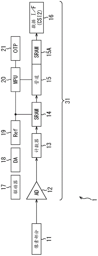
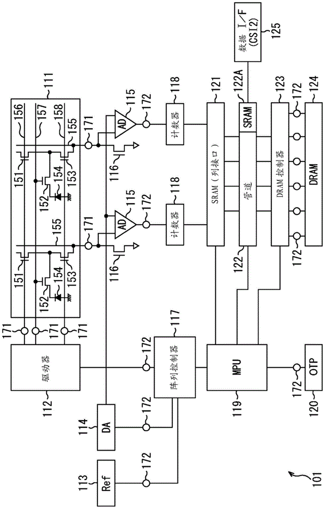
[0054] figure 2 is a block diagram showing a semiconductor device according to an embodiment of the present technology. A semiconductor device 101 usable as, for example, a CMOS image sensor (Complementary Metal Oxide Semiconductor Image Sensor) used in a digital camera includes a pixel portion 111 . A plurality of pixels that detect light from a subject are arranged in an n×m matrix in the pixel portion 111 . For convenience, in figure 2 Only two pixels are shown in .

[0055] Each pixel is composed of transistors 151 to 153 , and a photodiode 154 . The photodiode 154 outputs a video signal obtained by photoelectrically converting light from a subject. Transistor 152 transmits the video signal from photodiode 154 to transistor 153 . The transistor 153 amplifies the video signal supplied thereto from the photodiode 154 through the transistor 152 and outputs the resulting video signal to the line 155 . Transistor 151 selects the photodiode 154 to be driven.

[0056]The...


PUM


Abstract

A semiconductor device includes: a first substrate having a sensing portion detecting predetermined information; a second substrate having a first processing portion processing data supplied thereto from the sensing portion; and a third substrate having a second processing portion processing data supplied thereto either from the first substrate or from the second substrate.

Description

technical field [0001] The present technology relates to a semiconductor device and a sensing system including the semiconductor, and more particularly, to a semiconductor device capable of obtaining a high-quality signal, and a sensing system including the semiconductor. Background technique [0002] In proposing the technology of the present technology, differences between the existing semiconductor device and sensing system, and the semiconductor device and sensing system of the present technology will be described below. Hereinafter, a description will be given by illustrating an image processing sensing system. [0003] figure 1 is a block diagram showing an example of the configuration of a conventional image sensor 1 . In the existing image sensor 1 , the reference voltage generation section 19 supplies a necessary reference voltage to each of the respective sections. The driver 17 drives the pixel portion 11 in which a plurality of pixels are arranged in a matrix,...

Claims


Application Information

Patent Timeline
IPC IPC(8): H04N5/378H01L27/146
CPCH01L27/14609H01L27/1465H01L2924/0002H04N25/79H04N25/75H01L2924/00H04N25/60H01L25/167
Inventor G.阿萨亚马A.夏尔马
Owner SONY CORP
Why Eureka
Try Eureka