Optical filter device, optical module, electronic device, and MEMS device

An optical filter and interference filter technology, applied in the field of MEMS devices and optical filter devices, can solve the problems of MEMS components falling off, interference filter spectroscopic accuracy decline, interference filter falling off, etc., to achieve the effect of increasing fixing force

Inactive Publication Date: 2015-04-15
SEIKO EPSON CORP
View PDF6 Cites 13 Cited by
  • Summary
  • Abstract
  • Description
  • Claims
  • Application Information

AI Technical Summary

Problems solved by technology

When the substrate is deflected, the reflective film provided on the substrate is distorted, or the size of the gap between the reflective films changes, and the spectral accuracy of the interference filter decreases.
[0005] On the other hand, if the fixed area of ​​the adhesive is reduced, the interference filter may come off from the case when vibration or shock is applied.
[0006] In the above-mentioned various MEMS devices, when the substrate constituting the MEMS element is deflected, the performance of the MEMS element is degraded due to the influence of the deflection
On the other hand, if the fixing area is reduced, there is the same problem of MEMS components falling out of the case

Method used


Image

  • Optical filter device, optical module, electronic device, and MEMS device
  • Optical filter device, optical module, electronic device, and MEMS device
  • Optical filter device, optical module, electronic device, and MEMS device

Examples


no. 1 approach

[0077]Hereinafter, a first embodiment according to the present invention will be described based on the drawings.

[0078] [Configuration of Optical Filter Device]

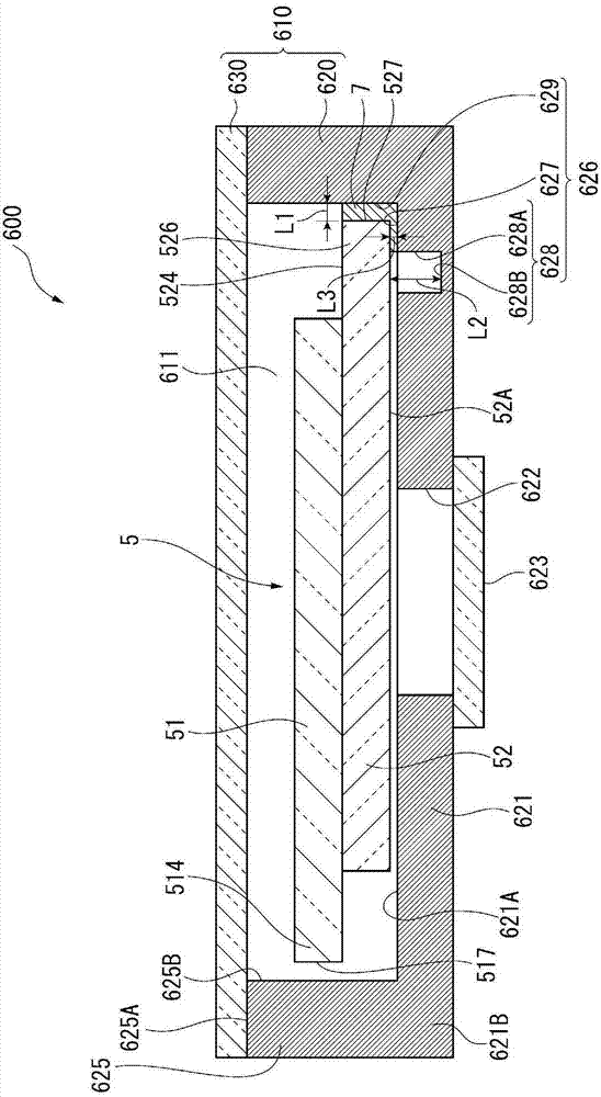
[0079] figure 1 It is a cross-sectional view showing a schematic configuration of an optical filter device 600 as one embodiment of the optical filter device of the present invention.

[0080] The optical filter device 600 is a device that extracts light of a predetermined target wavelength from incident light to be inspected and emits it, and includes: a housing 610 ; and a variable wavelength interference filter 5 housed inside the housing 610 . Such an optical filter device 600 can be incorporated into an optical module such as a colorimetric sensor, an electronic device such as a colorimetric device, or a gas analysis device, for example. In addition, the configuration of an optical module or electronic equipment including the optical filter device 600 will be described later.

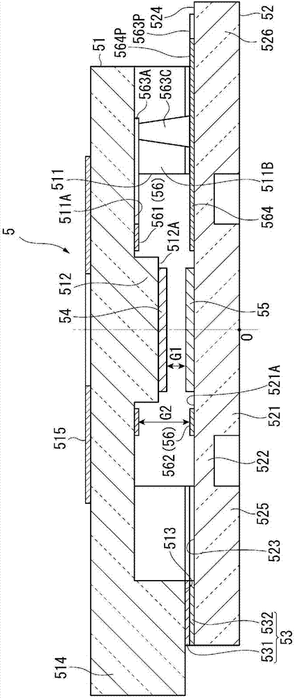
[0081] [Configuration of var...

no. 2 approach

[0155] Next, a second embodiment according to the present invention will be described based on the drawings.

[0156] In this embodiment, the bottom portion 620 is provided with a stepped portion at a position where the fixed substrate 51 overlaps with the protruding portion 514 in the filter plan view, and the fixed substrate 51 is fixed to the case 610 .

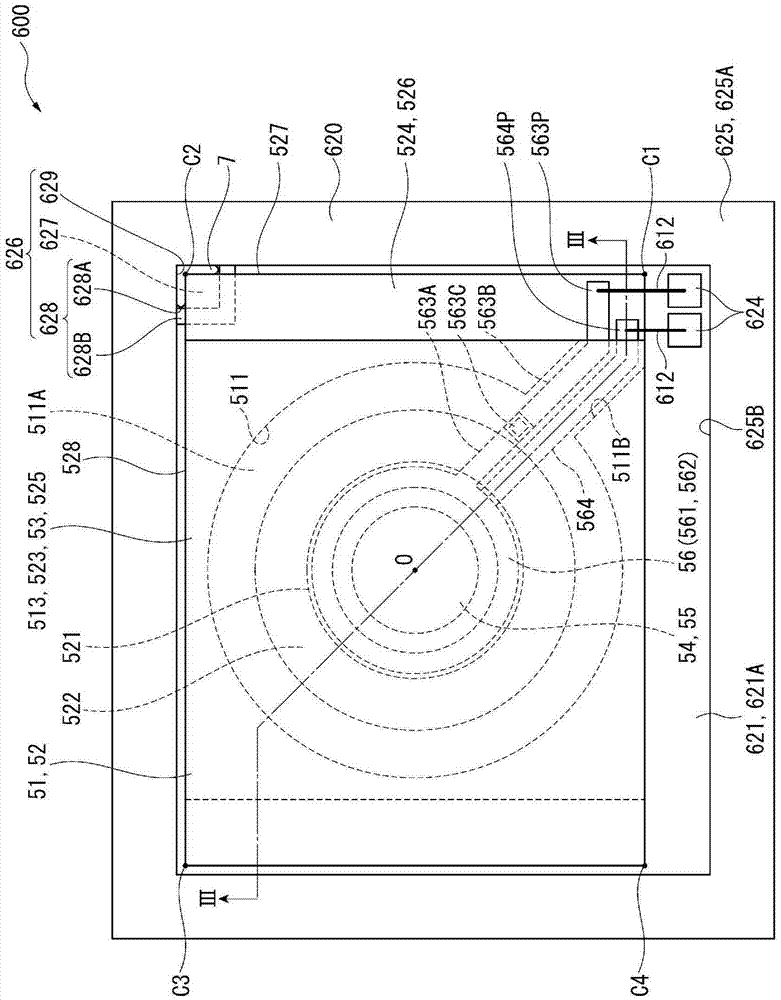
[0157] Figure 4 It is a cross-sectional view showing a schematic configuration of an optical filter device 600A according to a second embodiment of the present invention, Figure 5 It is a plan view showing a schematic configuration of the above-mentioned optical filter device 600A. In addition, in Figure 5 In , illustration of the cover 630 is omitted. In addition, in the following description, the same code|symbol is attached|subjected to the structure already demonstrated, and the description is abbreviate|omitted or simplified.

[0158] The optical filter device 600A includes a housing 610A and a variable wavelen...

no. 3 approach

[0180] Next, a third embodiment according to the present invention will be described based on the drawings.

[0181] In the third embodiment, the colorimetric sensor 3 which is an optical module incorporating the optical filter device 600 of the first embodiment described above, and the colorimetric device 1 which is an electronic device incorporating the optical filter device 600 will be described.

[0182] [Schematic configuration of the colorimetric device]

[0183] Image 6 It is a block diagram showing a schematic configuration of the colorimetric device 1 .

[0184] The colorimetric device 1 is the electronic device of the present invention. The colorimetric device 1 such as Image 6 As shown, a light source device 2 for emitting light toward an inspection object X, a colorimetric sensor 3 , and a control device 4 for controlling the overall operation of the colorimetric device 1 are provided. In addition, in this colorimetric device 1 , the inspection object light e...


PUM


Abstract

An optical filter device includes a wavelength variable interference filter, a housing that stores the wavelength variable interference filter, and a bonding member that fixes a movable substrate to the housing. The housing includes a fixing portion that comes into contact with the bonding member, the fixing portion includes a pedestal fixing surface (first surface) facing a portion of a surface of the movable substrate, a sidewall fixing surface (second surface), continuous with a portion of a periphery of the pedestal fixing surface, which faces a lateral side of the movable substrate, and an intersection surface (third surface) continuous from a remaining portion in a periphery of the pedestal fixing surface in a direction away from the movable substrate, and the bonding member is provided between the substrate surface and the pedestal fixing surface, and between the lateral side and the sidewall fixing surface.

Description

technical field [0001] The present invention relates to an optical filter device, an optical module, electronic equipment and a MEMS device. Background technique [0002] Conventionally, there are known interference filters in which reflective films are disposed opposite to each other on the opposing surfaces of a pair of substrates via a predetermined gap, mirror elements in which reflective films are disposed on the substrates, and piezoelectric elements such as crystal resonators disposed on the substrates. Various MEMS (Micro Electro Mechanical Systems (Micro Electro Mechanical Systems)) components such as piezoelectric vibration elements on the surface. In addition, there is known a MEMS device in which such a MEMS element is accommodated in a storage container (for example, refer to Patent Document 1). [0003] Patent Document 1 describes an infrared gas detector (optical filter device) including a unit (casing) including a plate-shaped base and a cylindrical cover. ...

Claims


Application Information

Patent Timeline
Patent Type & Authority Applications(China)
IPC IPC(8): G02B26/00G02B5/28
CPCG02B5/284B81B5/00G02B26/001
Inventor 松野靖史斋藤大辅今井英生小池繁光
Owner SEIKO EPSON CORP
Why Eureka
Try Eureka