Formation method of digital micro display

A digital micromirror device and device technology, applied in instruments, optical components, optics, etc., can solve the problems of inability to remove the patterned photoresist layer, and the inability to remove the hinge patterned photoresist layer. Body damage, shortened time, improved performance

Active Publication Date: 2015-04-15
SEMICON MFG INT (SHANGHAI) CORP
View PDF4 Cites 0 Cited by
  • Summary
  • Abstract
  • Description
  • Claims
  • Application Information

AI Technical Summary

Problems solved by technology

[0013] The problem to be solved by the present invention is: the existing digital micromirror device formation method cannot completely remove the patterned photoresist layer above the hinge
[0014] Another problem to be solved by the present invention is: the existing digital micromirror device formation method cannot completely remove the patterned photoresist layer above the fixed electrode

Method used


Image

  • Formation method of digital micro display
  • Formation method of digital micro display
  • Formation method of digital micro display

Examples


Embodiment Construction

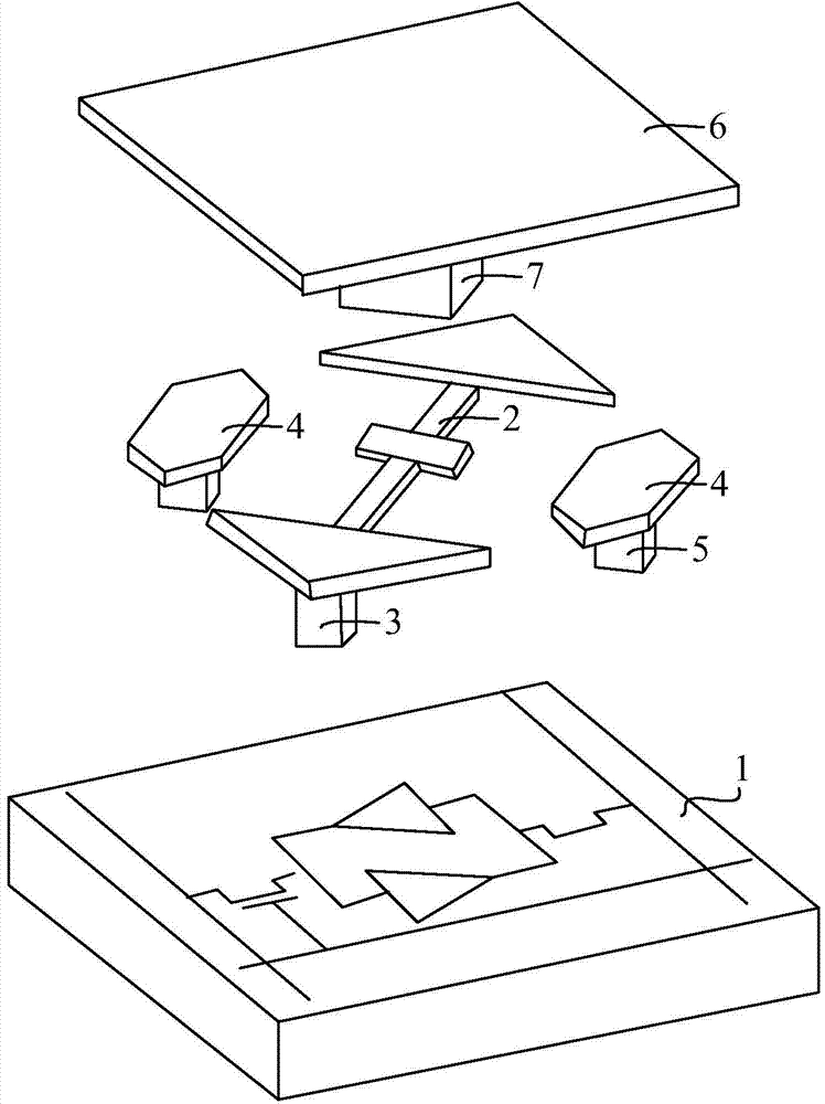
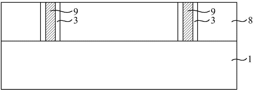
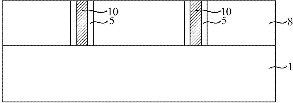
[0048] After research and analysis, it is found that the reason why the existing digital micromirror device formation method cannot remove the patterned photoresist layer above the hinge is: Figure 5A and Figure 5B As shown, the patterned photoresist layer 11 is used to protect the dielectric layer 22 in the hinge 2, so that the dielectric layer 22 will not be etched during the process of forming the hinge 2 by dry etching. In order to make the patterned photoresist layer 11 can play this role, it is necessary to ensure that the patterned photoresist layer 11 has sufficient thickness; Figure 6A and Figure 6B As shown, in the step of removing the patterned photoresist layer 11 by using the wet etching method, in order to enable the patterned photoresist layer 11 to be removed cleanly, it is necessary to ensure that the wet etching takes a long time, but in this way It will cause the two ends of the dielectric layer 22 in the hinge 2 to be corroded by the etchant. In order...


PUM

PropertyMeasurementUnit
thicknessaaaaaaaaaa
thicknessaaaaaaaaaa

Abstract

Disclosed is a formation method of a digital micro display. The method includes: providing a substrate with a micro display control circuit formed thereon; forming a first sacrificial layer on the substrate; forming a conducting material layer, a dielectric material layer on the conducting material layer and a pattern photoresist layer located on the dielectric material layer on the first sacrificial layer; by taking the pattern photoresist layer as a mask, performing dry etching on the dielectric material layer and the conducting material layer so as to form a hinge; after the hinge is formed, removing part of the pattern photoresist layer by means of wet etching; performing anisotropic dry etching on the rest part of the pattern photoresist layer. The whole pattern photoresist layer is removed cleanly, meanwhile the first sacrificial layer under the hinge cannot be corroded so as to avoid collapse of the hinge, the dielectric layer of the hinge is protected against etching, and the plasma damage to the substrate is reduced as well.

Description

technical field [0001] The invention relates to the technical field of semiconductors, in particular to a method for forming a digital micromirror device. Background technique [0002] Digital Micro Display (DMD) is a new type of all-digital flat panel display device, which integrates a reflective micromirror array and CMOS SRAM on the same chip. Since the reflective micromirror occupies most of the display area of ​​the digital micromirror device unit, a system with high brightness and high image quality can be produced. [0003] figure 1 It is an exploded view of the three-dimensional structure of an existing digital micromirror device, such as figure 1 As shown, the digital micromirror device includes: a substrate 1, a micromirror device control circuit is formed on the substrate 1; a digital micromirror array on the substrate 1, and each digital micromirror in the digital micromirror array includes: through two A hinge (hinge) 2 above the base 1 is supported by a firs...

Claims


Application Information

Patent Timeline
Patent Type & Authority Applications(China)
IPC IPC(8): G02B26/08
Inventor 伏广才汪新学倪梁
Owner SEMICON MFG INT (SHANGHAI) CORP
Why Eureka
Try Eureka