

Ring removing method of Taiko thinning process
A technology, the technology of Taiko, which is applied in the ring removal field of the Taiko thinning process, can solve the problems of edge chipping, wafer breaking, fragmentation, etc.
- Summary
- Abstract
- Description
- Claims
- Application Information
AI Technical Summary
Problems solved by technology
Method used
Image

Examples
Embodiment Construction
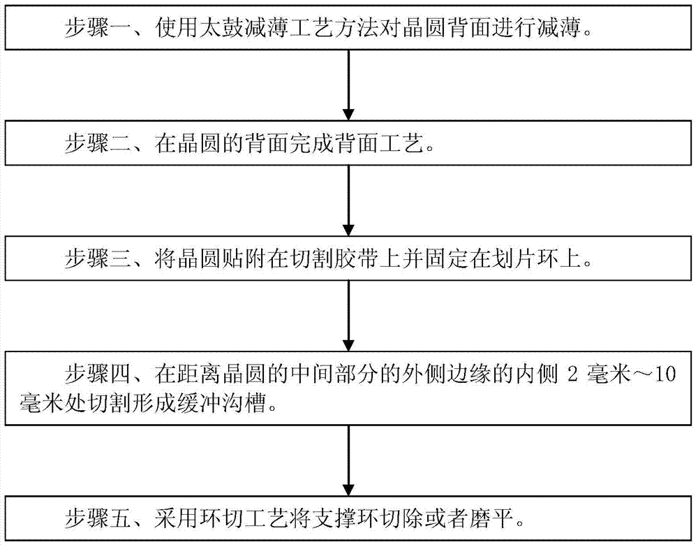
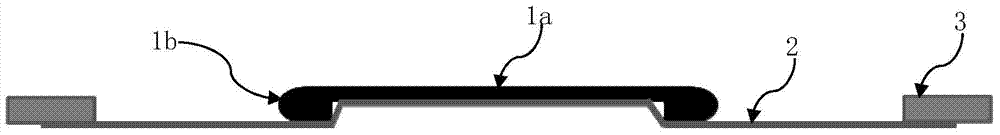
[0026] Such as figure 1 Shown is the flow chart of the method of the embodiment of the present invention; Figure 2A to Figure 2D Shown is a schematic diagram of the wafer structure in each step of the method of the embodiment of the present invention. The deringing method of Taiko drum thinning process in the embodiment of the present invention comprises the following steps:
[0027] Step 1, such as Figure 2A As shown, the back of the wafer is thinned using the Taiko thinning process, the middle portion 1a of the wafer is thinned to a required thickness, and the edge portion of the wafer is not thinned to form a support ring 1b.
[0028] The middle portion 1a of the wafer is used to form integrated circuit devices. Preferably, the thickness of the middle part 1a of the wafer after backside thinning is 25 microns to 200 microns, and the specific thickness can be adjusted according to the needs of integrated circuit devices.
[0029] The support ring 1b is used to support ...
PUM
| Property | Measurement | Unit |
|---|---|---|
| Width | aaaaa | aaaaa |
| Width | aaaaa | aaaaa |
| Thickness | aaaaa | aaaaa |
Abstract
Description
Claims
Application Information