
PCBA solder joint inspection method based on machine vision

A technology of solder joint detection and machine vision, which is applied in the field of PCBA solder joint detection based on machine vision, can solve problems such as thinning tin, insufficient smoothness, and high labor costs, and achieve the goals of overcoming difficult resolution, improving detection efficiency, and reducing labor costs Effect

Inactive Publication Date: 2015-04-22
安徽禾元建筑劳务有限公司
View PDF17 Cites 21 Cited by
  • Summary
  • Abstract
  • Description
  • Claims
  • Application Information

AI Technical Summary

Problems solved by technology

However, due to factors such as dense distribution of solder joints and small volume in PCBA, there is currently no special solder joint detection technology, and it is often only a unified detection during functional testing
However, for the PCBA address line, if there is a solder joint short circuit, etc., the defect cannot be detected through the subsequent functional inspection, which will affect the effect of the product, but it is impossible to have a very fine test effect during production testing. , Therefore, this detection method is inefficient, and it is easy to miss detection, and the defective product is mixed into the finished product, which has an impact on product quality
[0004] In addition, in addition to adhesion and short circuit, solder joints are also prone to various situations such as thin tin, less tin, insufficient plumpness, or insufficient smoothness. These situations cannot be detected by functional testing, but they will directly affect the functional stability of the PCBA. performance and service life
[0005] At present, some solder joint inspections that must be carried out are mostly realized through manual visual inspection, which is inefficient, high in labor costs, and high in missed detection rates.

Method used


Image

  • PCBA solder joint inspection method based on machine vision

Examples


Embodiment Construction

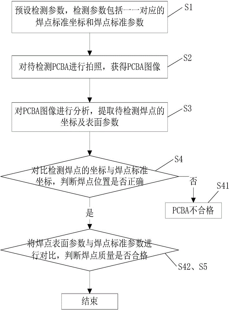
[0022] refer to figure 1 , a PCBA solder joint detection method based on machine vision proposed by the present invention, judges the position and quality of solder joints through image acquisition and analysis, with high accuracy and low labor cost.

[0023] A kind of PCBA solder spot detection method based on machine vision that the present invention proposes specifically comprises the following steps:

[0024] S1. Preset detection parameters. The detection parameters include one-to-one corresponding solder joint standard coordinates and solder joint standard parameters.

[0025] The solder joints are used to fix the components on the circuit board, so the positions of the solder joints on the same PCBA should be the same. Therefore, after selecting a fixed origin on the circuit board, the coordinates of the solder joints relative to the origin should be is consistent.

[0026] In this embodiment, the standard coordinates of the solder joints are the coordinates of the sol...


PUM


Abstract

The invention provides a PCBA solder joint inspection method based on machine vision. The solder joint position and quality are judged by virtue of image acquisition and analysis. The method specifically comprises the following steps: S1, presetting detection parameters, wherein the detection parameters comprise the solder joint standard coordinates and solder joint standard parameters which are in one-to-one correspondence; S2, photographing to-be-detected PCBA, thereby obtaining a PCBA image; S3, analyzing the PCBA image, and extracting the coordinate and surface parameters of the to-be-detected solder joint; S4, comparing the coordinates of the detected solder joint with the solder joint standard coordinates to and judge whether the solder joint position is accurate; and S5, comparing the solder joint surface parameters with the solder joint standard parameters according to the solder joint coordinates and the solder joint standard coordinates to judge whether the solder joint quality is qualified. According to the method disclosed by the invention, the solder joint detection is performed by utilizing the machine vision technology, the problems that the solder joints are high in intensity and difficult to distinguish, detection leakage is easily caused and the like are effectively solved, the solder joint detection accuracy is guaranteed, the detection efficiency is improved, and the labor cost is reduced.

Description

technical field [0001] The invention relates to the technical field of PCBA detection, in particular to a method for detecting PCBA solder joints based on machine vision. Background technique [0002] In today's manufacturing industry, packaging technology is often used to package PCBA boards. However, as the integration degree of PCBA (Printed Circuit Board+Assembly, circuit board assembly) board becomes higher, it becomes more and more difficult to detect the packaged circuit board. [0003] Many components in PCBA are welded by electric welding, so solder joint inspection is a very necessary inspection object in PCBA inspection. However, due to factors such as dense distribution of solder joints and small volume in PCBA, there is currently no special solder joint detection technology, and it is often only a unified detection during functional testing. However, for the PCBA address line, if there is a solder joint short circuit, etc., the defect cannot be detected throug...

Claims


Application Information

Patent Timeline
Patent Type & Authority Applications(China)
IPC IPC(8): G01N21/95
Inventor 吕月林
Owner 安徽禾元建筑劳务有限公司
Learn More