Display panel and display device

A technology for display panels and display devices, applied to instruments, static electricity, electrical components, etc., can solve the problems of high cost and complex production process, and achieve the effects of low production cost, reduction of production cost, and simplification of production process

Inactive Publication Date: 2015-04-22
SHANGHAI TIANMA MICRO ELECTRONICS CO LTD +1
View PDF6 Cites 32 Cited by
  • Summary
  • Abstract
  • Description
  • Claims
  • Application Information

AI Technical Summary

Problems solved by technology

The defect of this prior art is that the indium tin oxide thin film needs to be formed on the outside of the glass substrate of the color filter substrate by means of physical vapor deposition, the production process is relatively complicated, and the cost is relatively high

Method used


Image

  • Display panel and display device
  • Display panel and display device
  • Display panel and display device

Examples


Embodiment Construction

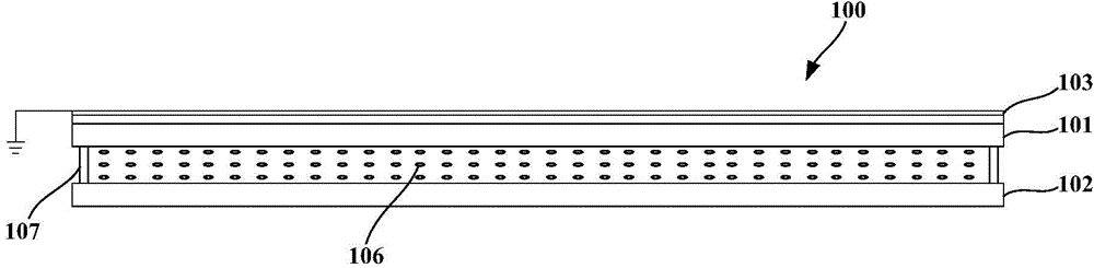
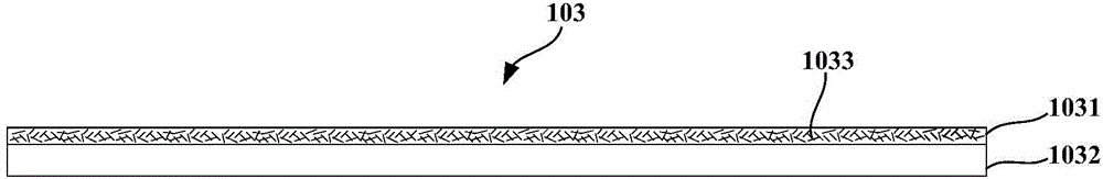
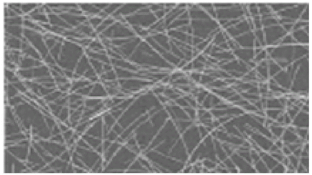
[0041] In order to simplify the production process of the display panel and reduce the production cost while enabling the display panel to have a better anti-static damage effect, embodiments of the present invention provide a display panel and a display device. In the technical solution of the embodiment of the present invention, the display panel includes a conductive layer disposed on the side of the first substrate facing away from the second substrate, the conductive layer is grounded, includes a base layer, and nano conductive materials disposed in the base layer. Since the conductive layer is conductive and grounded, the electrostatic charge on the display panel can be quickly exported to the ground, so that the display panel has a better anti-static damage effect; because the conductive layer is more flexible, it can be directly attached to the The surface of the first substrate facing away from the second substrate, so compared with the prior art, the solution can great...


PUM

PropertyMeasurementUnit
thicknessaaaaaaaaaa
thicknessaaaaaaaaaa
diameteraaaaaaaaaa

Abstract

The invention discloses a display panel and a display device. The display panel has the good anti-static-damage effect. Meanwhile, the production technology of the display panel is simplified, and production cost is reduced. The display panel comprises a first substrate, a second substrate and a conductive layer, wherein the first substrate and the second substrate are oppositely arranged, and the conductive layer is arranged on the side, opposite to the second substrate, of the first substrate. The conductive layer is grounded and comprises a base layer and a nano conductive material arranged in the base layer. Due to the fact that the conductive layer has the electric conductibility and is grounded, static charges on the display panel can be rapidly led out and led into the ground, and the display panel has the good anti-static-damage effect. Due to the good flexibility of the conductive layer, the conductive layer can be directly attached to the surface of the side, opposite to the second substrate, of the first substrate; in this way, the production technology of the display panel can be greatly simplified, production cost is reduced, and the anti-static-damage capacity of the display panel can be greatly improved.

Description

Technical field [0001] The present invention relates to the field of display technology, in particular to a display panel and a display device. Background technique [0002] Among the flat panel display devices, Thin Film Transistor Liquid Crystal Display (TFT-LCD) has the characteristics of small size, low power consumption, relatively low manufacturing cost, and no radiation, and it is dominant in the current flat panel display market. status. The structure of TFT-LCD mainly includes: a display panel and a backlight source located below the display panel; among them, the display panel includes an array substrate and a color film substrate that are boxed by a frame sealant, and a filling between the array substrate and the color film substrate liquid crystal. [0003] Electrostatic discharge ESD (Electro Static Discharge) refers to the transfer of electrostatic charge between objects caused by direct contact or electrostatic induction of objects with different electrostatic pote...

Claims


Application Information

Patent Timeline
Patent Type & Authority Applications(China)
IPC IPC(8): G02F1/1333H05F3/02
CPCG02F1/136204G02F1/1333H05F3/02
Inventor 孙晓平王丽花佘晓飞任玉萍
Owner SHANGHAI TIANMA MICRO ELECTRONICS CO LTD
Why Eureka
Try Eureka