

Core-less board manufacturing method
A manufacturing method and coreless board technology, which can be used in printed circuit manufacturing, multi-layer circuit manufacturing, semiconductor/solid-state device manufacturing, etc. The effect of increasing the pressing temperature and reducing the warpage
- Summary
- Abstract
- Description
- Claims
- Application Information
AI Technical Summary
Problems solved by technology
Method used
Image

Examples
Embodiment 1
[0039]
Embodiment 2
[0041]
Embodiment 3
4.9mm
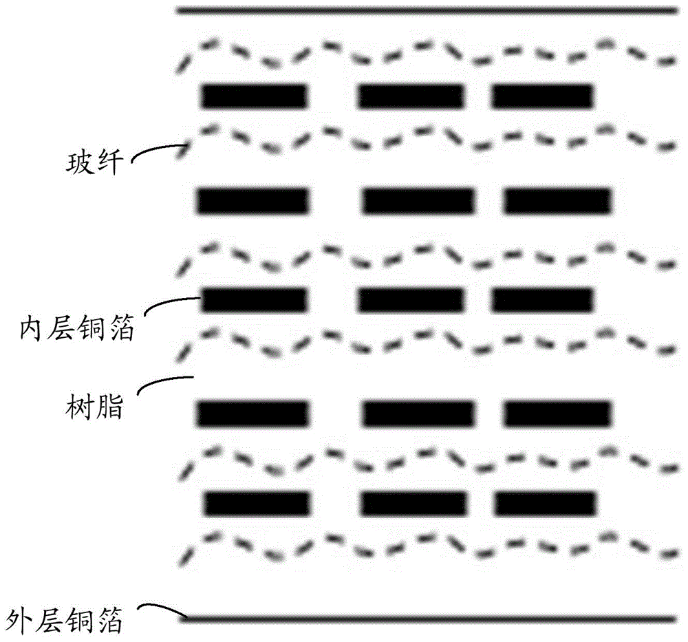
[0045] The warpage height refers to the height difference between the two ends of the coreless board; the warpage rate is the value of the height difference divided by the length of the board to represent the degree of warpage of the board.
[0046] The above examples all show that controlling the glass fiber thickness difference between the outer curing sheet and the inner curing sheet to be greater than 8 μm can effectively control the warpage rate below 1%, and the warpage height difference is not higher than 5mm. And the greater the difference in glass fiber thickness, the lower the warpage rate.
[0047] By asymmetrically adjusting and matching the glass fiber thickness and resin content of different layers of prepreg, the warpage reduction of the coreless board can be achieved simply and at low cost.
[0048] In addition, a double-layer glass fiber structure can also be arranged inside the outer curing sheet. The double-layer glass fiber structure inclu...
PUM
| Property | Measurement | Unit |
|---|---|---|
| thickness | aaaaa | aaaaa |
Abstract
Description
Claims
Application Information