Supercharge Your Innovation With Domain-Expert AI Agents!

Display panel, manufacturing method thereof, and display device

A display panel and insulating layer technology, which is applied in semiconductor/solid-state device manufacturing, semiconductor/solid-state device components, semiconductor devices, etc., can solve the problem of defective display panels, exposed pin signal lines, and vias that cannot drive the pins of the chip Complete package and other problems, to achieve the effect of simple process, easy implementation and good display quality

Inactive Publication Date: 2017-11-10
BOE TECH GRP CO LTD +1
View PDF5 Cites 0 Cited by
  • Summary
  • Abstract
  • Description
  • Claims
  • Application Information

AI Technical Summary

Problems solved by technology

[0005] The technical problems to be solved by the present invention include, aiming at the existing problems of the via holes in the fan-out area of ​​the display panel, to provide an effective method to improve the problem that the pins of the driver chip cannot be completely wrapped due to the large via holes, which in turn leads to tube Defective display panel caused by exposed signal lines under feet, manufacturing method thereof, and display device

Method used


Image

  • Display panel, manufacturing method thereof, and display device
  • Display panel, manufacturing method thereof, and display device
  • Display panel, manufacturing method thereof, and display device

Examples


Embodiment 1

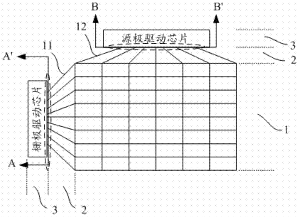
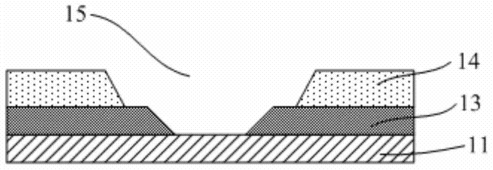
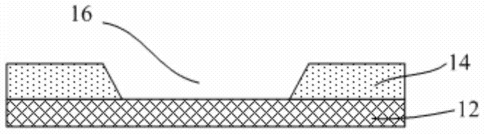
[0049] This embodiment provides a display panel, which includes a pixel area, a fan-out area, and a driving circuit area, and the fan-out area is arranged between the pixel area and the driving circuit area; wherein, a first signal line and a second Two signal lines, the first signal line and the second signal line both extend to the fan-out area; the first driver chip and the second driver chip are arranged in the driver circuit area; the layer where the first signal line and the second signal line are located A first insulating layer is arranged between them, and a second insulating layer is arranged above the second signal line; the first driver chip passes through the first insulating layer and the second insulating layer above the first signal line in the fan-out area. The first via hole is electrically connected to the first signal line; the second driver chip is electrically connected to the second signal line through the second via hole penetrating through the second in...

Embodiment 2

[0058] This embodiment provides a method for manufacturing a display panel, wherein the display panel may be the display panel described in Embodiment 1.

[0059]Wherein, the display panel includes a pixel area, a fan-out area and a driving circuit area, and the fan-out area is arranged between the pixel area and the driving circuit area; the pixel area includes a plurality of cross-arranged first signals line and a second signal line, the first signal line and the second signal line both extend to the fan-out area, a first insulating layer is arranged between the first signal line and the second signal line, and the second signal line A second insulating layer is arranged above the line, and the second insulating layer includes at least four-layer structure, and the density of each layer structure gradually decreases along the direction away from the first insulating layer; the driving circuit area includes a plurality of first insulating layers. a driver chip and a plurality...

Embodiment 3

[0078] This embodiment provides a display device, which includes the display panel described in Embodiment 1, so it has better performance and higher yield.

[0079] The display device provided by the present invention may be a liquid crystal display device of any mode such as TN, ADS, IPS, LTPS and the like. The display device can be any product or component with a display function, such as a liquid crystal panel, a liquid crystal TV, a monitor, a mobile phone, a navigator, and the like.


PUM


Abstract

The invention provides a display panel, a preparation method thereof, and a display device, which belong to the field of display technology and can solve the problem of large via holes in the fan-out area of ​​the existing display panel. The display panel of the present invention includes: a pixel area and a fan-out area, the pixel area includes a plurality of first signal lines and second signal lines intersecting, and the first signal lines and the second signal lines both extend to In the fan-out area, a first insulating layer is disposed between the first signal line and the second signal line, and a second insulating layer is disposed above the second signal line, the second insulating layer includes at least four layers, and each The density of the layer structure gradually decreases in a direction away from the first insulating layer. Since the second insulating layer of the present invention adopts the above structure, the via hole formed after etching is smaller than the existing via hole.

Description

technical field [0001] The invention belongs to the field of display technology, and in particular relates to a display panel, a preparation method thereof, and a display device. Background technique [0002] The flat panel display is currently the main popular display, which is widely used in computer screens, mobile phones and other electronic products due to its thin and light appearance, power saving and no radiation. [0003] The display panel is the main component of a flat panel display, such as figure 1 As shown, the display panel includes a pixel area 1, a fan-out area 2, and a driving circuit area 3; wherein, the pixel area 1 includes a plurality of cross-arranged gate lines 11 and data lines 12, and between the gate lines 11 and the data lines 12 A first insulating layer 13 (usually a gate insulating layer) is provided, and a second insulating layer 14 (usually a passivation layer) is provided above the data lines 12, and these gate lines 11 and data lines 12 bot...

Claims


Application Information

Patent Timeline
Patent Type & Authority Patents(China)
IPC IPC(8): H01L27/12H01L23/528H01L21/77H01L21/768
CPCH01L21/76804H10K59/124H01L21/02271H01L21/76802H01L25/0655H01L25/50H01L27/124H01L27/1259
Inventor 李婧崔玉琳
Owner BOE TECH GRP CO LTD
Features
  • R&D
  • Intellectual Property
  • Life Sciences
  • Materials
  • Tech Scout
  • Unparalleled Data Quality
  • Higher Quality Content
  • 60% Fewer Hallucinations
Learn More