High-reliability fully-closed CMOS image sensor structure and production method thereof

A technology of image sensor and image sensor chip, which is applied in the direction of radiation control devices, etc., to achieve the effects of improving anti-interference ability, good moisture insulation, and enhancing reliability

Active Publication Date: 2015-04-22
HUATIAN TECH KUNSHAN ELECTRONICS
View PDF6 Cites 10 Cited by
  • Summary
  • Abstract
  • Description
  • Claims
  • Application Information

AI Technical Summary

Problems solved by technology

[0004] However, they are suitable for use in the environment. If they further enter the application fields such as automobiles, exploration, and outdoor monitoring, higher requirements must be placed on the sensitivity, reliability, and durability of CMOS image sensors to withstand the test of harsh environments.

Method used


Image

  • High-reliability fully-closed CMOS image sensor structure and production method thereof
  • High-reliability fully-closed CMOS image sensor structure and production method thereof
  • High-reliability fully-closed CMOS image sensor structure and production method thereof

Examples


Embodiment Construction

[0055] In order to make the present invention more obvious and understandable, the specific implementation manners of the present invention will be described in detail below in conjunction with the accompanying drawings. For convenience of description, the components in the structures in the drawings of the embodiments are not scaled according to the normal scale, so they do not represent the actual relative sizes of the structures in the embodiments.

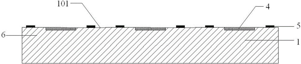
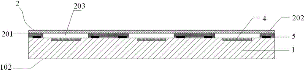
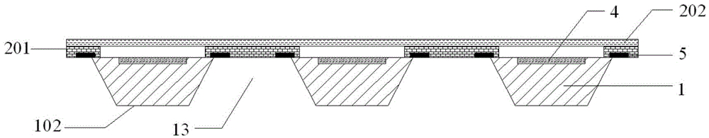
[0056] like Figure 10 As shown, a high-reliability fully enclosed CMOS image sensor structure includes an image sensor chip 3, the image sensor chip has a first surface 301 and a second surface 302 opposite thereto, and the first surface includes an image sensor area (4) and several welding pads 5 located at the periphery of the image sensing area; the first surface is bonded with a protective cover structure 2, and the protective cover structure includes a light-transmitting cover plate 202 and is arranged on the first surfac...


PUM


Abstract

The invention discloses a high-reliability fully-closed CMOS image sensor structure and a production method thereof. The structure comprises an image sensor chip, openings, a metal wiring layer, a plurality of solder bumps and a plastic package layer, wherein the openings are formed by extending from a second surface of the chip to a first surface, and a welding pad of the chip is exposed out of the bottoms of the openings; the metal wiring layer is positioned on the inner walls of the openings and the second surface of the image sensor chip, and are electrically connected with the welding pad, and the solder bumps are positioned on the second surface and are electrically connected with the metal wiring layer; the image sensor chip is coated by the plastic package layer, and an image induction zone and the solder bumps are exposed. The chip is protected by forming the whole plastic package layer, and the plastic package layer adopts a plastic package material with good moisture insulation, corrosion prevention or mechanical strength properties. The high-reliability fully-closed CMOS image sensor structure provided by the invention has the advantages of further enhancing the reliability and durability of the CMOS image sensor, enhancing the anti-interference ability of the image sensor chip, and meeting the application requirements on the CMOS image sensor in harsh environments.

Description

technical field [0001] The invention relates to the packaging field of CMOS image sensors, in particular to a highly reliable fully enclosed CMOS image sensor structure and a manufacturing method thereof. Background technique [0002] With the continuous improvement and improvement of CMOS integrated circuit technology in recent years, CMOS image sensor chips have been rapidly developed and widely used. Very popular. [0003] Figure 16 A known packaging structure of a CMOS image sensor is shown, including an image sensor chip 3, the functional surface of which image sensor chip includes an image sensing area 4 and several welding pads 5 around the image sensing area; an opening, the opening consists of The back extends toward the functional surface, and the bottom of the opening exposes the pad; the metal wiring layer 7, the metal wiring layer is located on the inner wall and the back of the opening, electrically connected to the pad; the insulating layer 6, the insulating...

Claims


Application Information

Patent Timeline
Patent Type & Authority Applications(China)
IPC IPC(8): H01L27/146
Inventor 万里兮黄小花王晔晔沈建树翟玲玲钱静娴
Owner HUATIAN TECH KUNSHAN ELECTRONICS
Why Eureka
Try Eureka