Optical proximity correction method

A technology of optical proximity correction and optical model, which is applied in the direction of optics, original components for photomechanical processing, instruments, etc., can solve problems such as unsatisfactory effects, achieve good effects and ensure physical effects

Active Publication Date: 2015-04-29
SEMICON MFG INT (SHANGHAI) CORP
View PDF8 Cites 8 Cited by
  • Summary
  • Abstract
  • Description
  • Claims
  • Application Information

AI Technical Summary

Problems solved by technology

[0007] However, the optimal value of each parameter obtained by the above optical p...

Method used


Image

  • Optical proximity correction method
  • Optical proximity correction method
  • Optical proximity correction method

Examples


Embodiment Construction

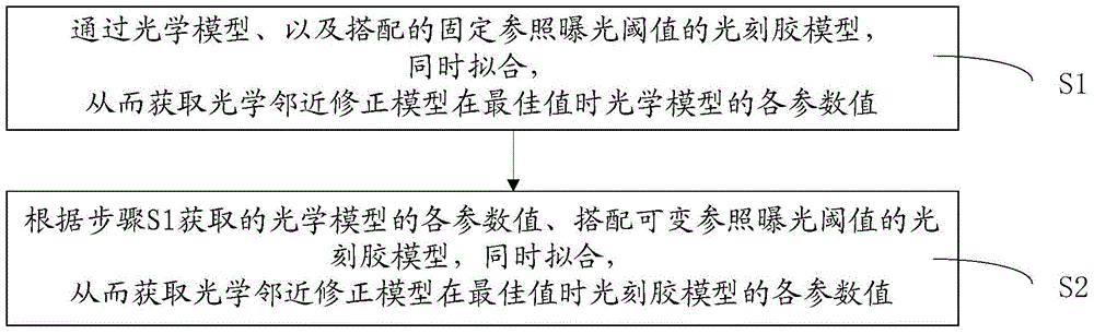
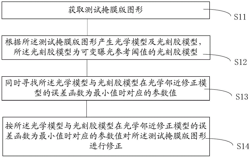
[0037] As mentioned in the Background Art, refer to figure 1 The parameters obtained by the existing optical proximity correction method shown are not ideal in the actual optical proximity correction process. After analysis, it is found that the reason is: through the optical model and the matching photoresist model (constant threshold resist model) with a fixed reference exposure threshold, the values ​​of the parameters of the optical model corresponding to the optimal value of the optical proximity correction model are only Focuses on the mathematical fitting process and does not consider the physical properties of the optical proximity correction model. In other words, the exposure reference threshold of the photoresist model corresponding to each parameter value in the optical model is not the same. Therefore, the optical proximity correction model obtained by using the photoresist model with a fixed exposure reference threshold corresponds to the optical model at the opt...


PUM


Abstract

The invention provides an optical proximity correction method. An optical model and a photoresist model of a variable exposed reference threshold value are fitted simultaneously to obtain an optimal correction parameter value for testing a mask pattern. According to the optical proximity correction method provided by the invention, the photoresist model does not depend on optical model parameters obtained by matching the inaccurate optical model with the photoresist model of the exposed reference threshold value so that the physical property of an optical proximity correction model is guaranteed and an obtained result is relatively close to actual optical proximity correction; and the effect of carrying out the optical proximity correction by adopting the result is relatively good.

Description

technical field [0001] The invention relates to the technical field of semiconductor manufacturing, in particular to an optical proximity correction method. Background technique [0002] Integrated circuit manufacturing technology is a complex process that will be updated every 18 to 24 months. A key parameter that characterizes integrated circuit manufacturing technology, the minimum feature size, that is, the critical dimension, has developed from the initial 125 microns to the current 0.13 microns or even smaller, which makes it possible to integrate millions of components on each chip. [0003] Photolithography is the driving force behind the development of integrated circuit manufacturing processes, and it is also one of the most complex technologies. Compared with other individual manufacturing technologies, photolithography has made a revolutionary contribution to the improvement of chip performance. Before the photolithography process starts, the structure of the i...

Claims


Application Information

Patent Timeline
IPC IPC(8): G03F1/36
CPCG03F1/36
Inventor 王辉
Owner SEMICON MFG INT (SHANGHAI) CORP
Why Eureka
Try Eureka