Silicon slice prealignment device and method

A pre-aligned, silicon wafer technology, used in electrical components, semiconductor/solid-state device manufacturing, circuits, etc., can solve problems such as inaccurate positioning, and achieve the effect of eliminating interference and improving accuracy

Active Publication Date: 2015-04-29
SHANGHAI MICRO ELECTRONICS EQUIP (GRP) CO LTD
View PDF6 Cites 5 Cited by
  • Summary
  • Abstract
  • Description
  • Claims
  • Application Information

AI Technical Summary

Problems solved by technology

[0004] The present invention provides a silicon chip pre-alignment device and its method to solve the problem that the existing silicon chip pre-alignment method is easily affected by the interference thread on the surface of the suction cup, resulting in inaccurate positioning

Method used


Image

  • Silicon slice prealignment device and method
  • Silicon slice prealignment device and method
  • Silicon slice prealignment device and method

Examples


Embodiment Construction

[0035] In order to describe the technical solutions of the above invention in more detail, specific embodiments are listed below to prove the technical effect; it should be emphasized that these embodiments are used to illustrate the present invention and not limit the scope of the present invention.

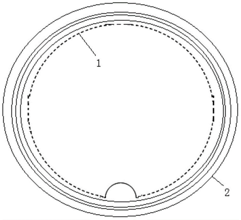
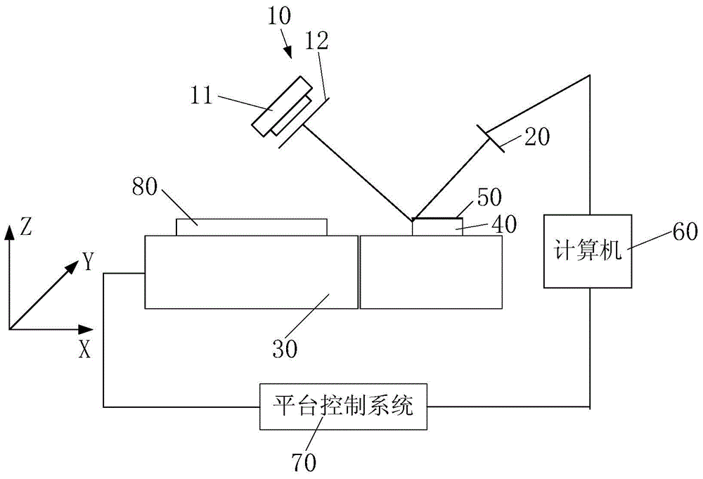
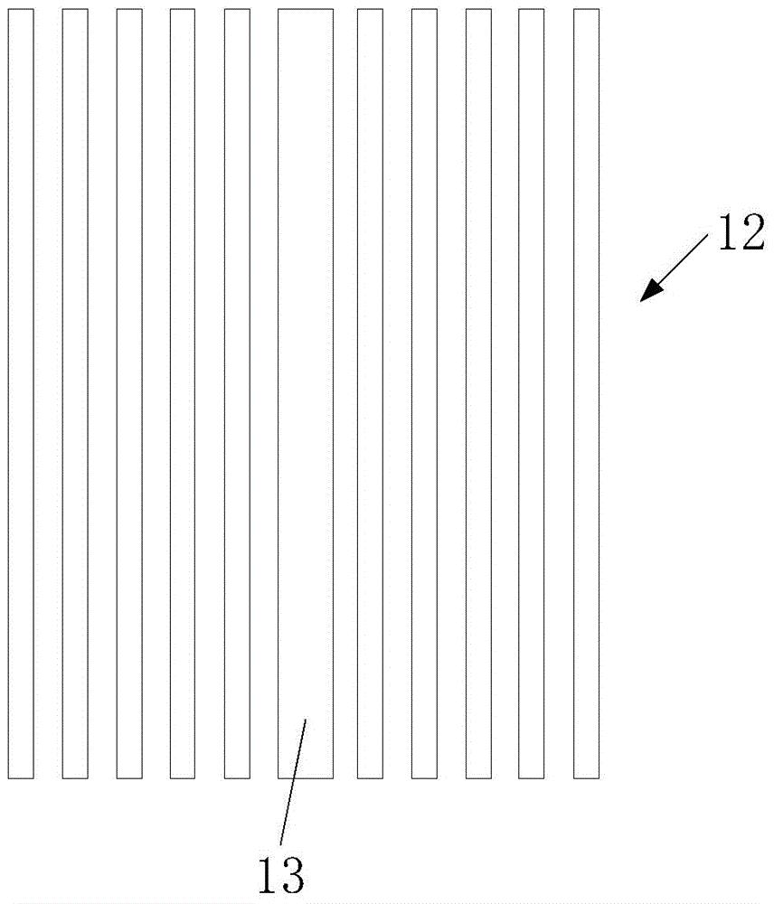
[0036] The silicon wafer pre-alignment device and method thereof provided by the present invention, such as figure 2 As shown, the device includes a structured light emission system 10, an imaging system 20, a workpiece table 30, a reference plate 40, a marker plate 50, a computer 60, and a platform control system 70. The silicon wafer 80 and the reference plate 40 are placed on the workpiece table, respectively. 30, the marking plate 50 is placed on the reference plate 40, the projection beam emitted by the structured light emission system 10 is irradiated to the edge of the reference plate 40, and the detection beam reflected by the projection beam is captured by the imaging s...


PUM


Abstract

The invention relates to a silicon slice prealignment device and method. The device comprises a structured light emission system, an imaging system, a workpiece table, a reference plate, a marking plate, a computer and a platform control system, wherein a silicon slice and the reference plate are respectively placed on the workpiece table; the marking plate is arranged on the reference plate; projection light beams emitted by the structured light emission system irradiate the edge of the reference plate; detection light beams reflected from the projection light beams are received by the imaging system; the imaging system, the computer, the platform control system and the workpiece table are connected in sequence. According to the silicon slice prealignment device, by the arrangement of the structured light emission system and the imaging system, three-dimensional coordinates of the edge of the silicon slice and the background of a sucker are determined, and then silicon slice edge points for subsequent software processing are accurately positioned; therefore, interference of non silicon slice edge points on the positioning of the center of the silicon slice is avoided, and the precision of a silicon slice prealignment system is improved.

Description

technical field [0001] The invention relates to a laser annealing machine system, in particular to a silicon wafer pre-alignment device and a method thereof. Background technique [0002] The silicon wafer pre-alignment system is one of the key sub-systems of the laser annealing machine system. Its main function is to calculate the position of the silicon wafer center in the coordinate system of the silicon wafer workpiece table, so as to detect the current position and attitude of the silicon wafer, which is used for the subsequent laser Annealing provides convenience. The positional deviation of the silicon wafer in the box may cause uneven annealing of the silicon wafer, so the alignment of the silicon wafer must be realized inside the equipment. [0003] The common silicon wafer alignment system is photographed by visible light illumination to obtain a picture of the edge of the silicon wafer, and the picture is processed by a software algorithm and positioned. Since t...

Claims


Application Information

Patent Timeline
Patent Type & Authority Applications(China)
IPC IPC(8): H01L21/68
CPCH01L21/324H01L21/681
Inventor 於陈慧杜荣
Owner SHANGHAI MICRO ELECTRONICS EQUIP (GRP) CO LTD
Why Eureka
Try Eureka