Preparation method of Trench IGBT with reverse conducting structure

A technology of reverse conduction and front structure, which is applied in semiconductor/solid-state device manufacturing, semiconductor devices, electrical components, etc., and can solve problems such as high requirements and complicated Trench IGBT process

Active Publication Date: 2015-04-29
CSMC TECH FAB2 CO LTD
View PDF6 Cites 4 Cited by
  • Summary
  • Abstract
  • Description
  • Claims
  • Application Information

AI Technical Summary

Problems solved by technology

[0004] The traditional preparation method of Trench IGBT with reverse conduction structure is complex and requires a thinner device. It requires high equipment requirements for steps such as backside lithography and development, and requires ultra-thin sheet lithography, development and other lithography equipment. factory hard to reach

Method used


Image

  • Preparation method of Trench IGBT with reverse conducting structure
  • Preparation method of Trench IGBT with reverse conducting structure
  • Preparation method of Trench IGBT with reverse conducting structure

Examples


Embodiment Construction

[0028] In order to make the above objects, features and advantages of the present invention more comprehensible, specific implementations of the present invention will be described in detail below in conjunction with the accompanying drawings. In the following description, numerous specific details are set forth in order to provide a thorough understanding of the present invention. However, the present invention can be implemented in many other ways different from those described here, and those skilled in the art can make similar improvements without departing from the connotation of the present invention, so the present invention is not limited by the specific implementations disclosed below.

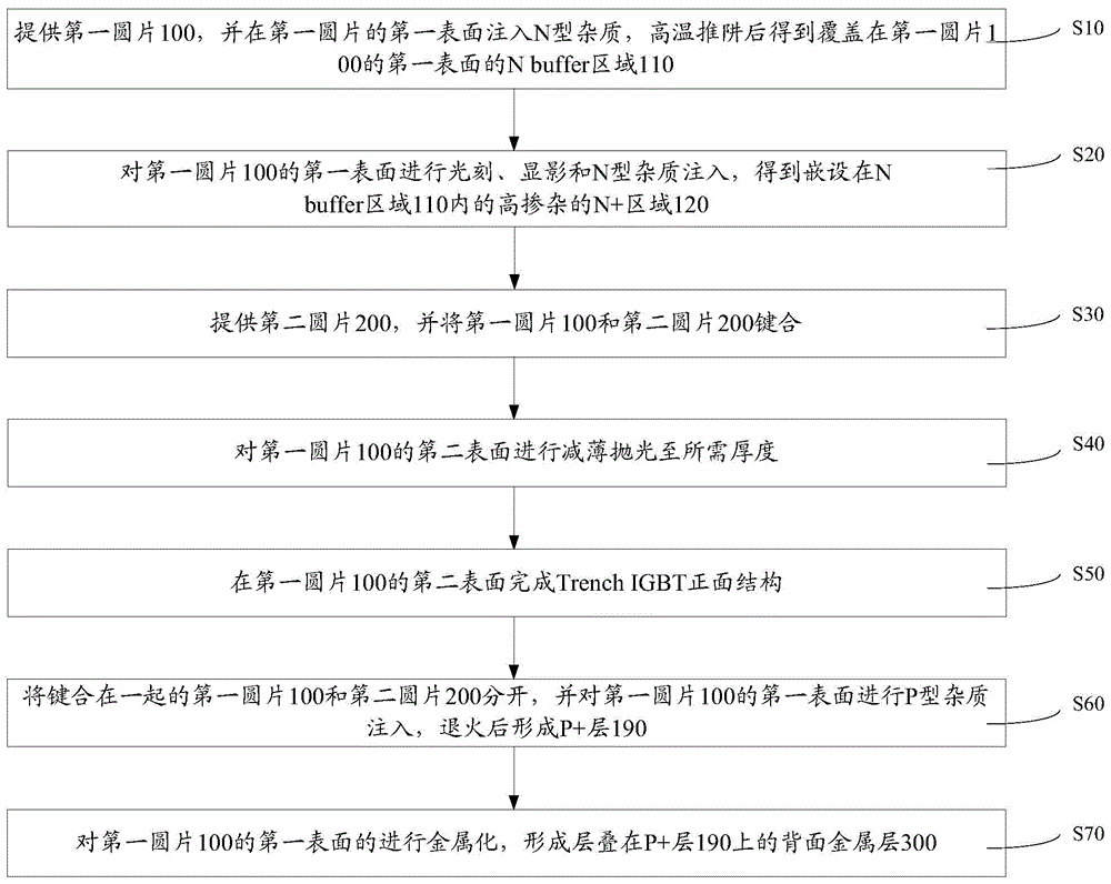
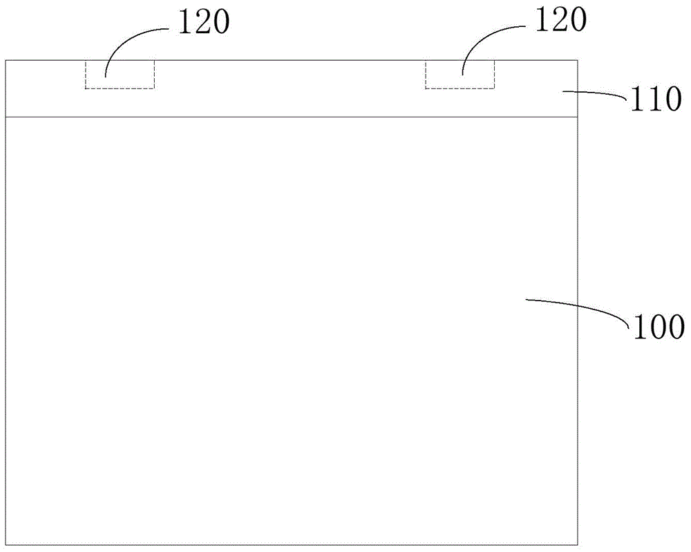
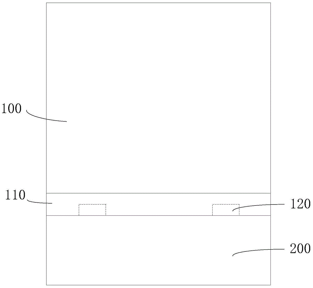
[0029] Such as figure 1 and Figure 2a ~ Figure 2d As shown, a Trench IGBT with a reverse conducting structure of an embodiment includes the following steps:

[0030] S10 , providing the first wafer 100 , and implanting N-type impurities on the first surface of the first wafer, and ...


PUM


Abstract

The invention discloses a preparation method of a Trench IGBT with a reverse conducting structure. The preparation method comprises the following steps: providing a first wafer, and forming an N buffer area and a highly doped N+ area in sequence on the first surface of the first wafer; providing a second wafer, and bonding the first wafer and the second wafer, wherein the first surface of the first wafer is in direct contact with the second wafer; carrying out thinning polishing on the second surface of the first wafer to required thickness; completing a Trench IGBT front-side structure on the second surface of the first wafer; separating the first wafer and the second wafer, which are bonded together, and forming a P+ layer and a back metal layer in sequence on the first surface of the first wafer. According to the preparation method of the Trench IGBT with the reverse conducting structure, through the bonding of the first wafer and the second wafer, firstly thinning is carried out, and then the Trench IGBT front-side structure is completed, so that photoetching or developing equipment for an ultrathin piece is not needed, and the process is simple.

Description

technical field [0001] The invention relates to the field of semiconductor manufacturing and processing, in particular to a method for preparing a Trench IGBT with a reverse conduction structure. Background technique [0002] Insulated Gate Bipolar Transistor (Insulated Gate Bipolar Transistor, IGBT) is a device composed of a MOSFET and a bipolar transistor. Its input is a MOSFET and its output is a PNP transistor. Therefore, the IGBT can be regarded as a Darlington tube with MOS input. IGBT not only has the advantages of MOSFET device voltage drive, high withstand voltage, simple drive, and fast switching speed, but also has the advantages of strong current capability and reduced conduction voltage of bipolar devices, so it has been more and more popular in modern power electronics technology. more and more widely used. [0003] The traditional preparation method of Trench Insulated Gate Bipolar Transistor (Trench IGBT) with reverse conducting structure generally thins th...

Claims


Application Information

Patent Timeline
Patent Type & Authority Applications(China)
IPC IPC(8): H01L21/8222H01L21/331
CPCH01L29/66348
Inventor 邓小社芮强张硕王根毅
Owner CSMC TECH FAB2 CO LTD
Why Eureka
Try Eureka