Wafer seat

A technology of wafer seat and crystal seat, which is applied in the direction of electrical components, electric solid devices, circuits, etc., can solve the problems of disengagement, difficulty in chip and wafer seat, fixation, etc., and achieve the effect of increasing adhesion

Inactive Publication Date: 2015-04-29
WUXI KENUODA ELECTRONICS
View PDF0 Cites 0 Cited by
  • Summary
  • Abstract
  • Description
  • Claims
  • Application Information

AI Technical Summary

Problems solved by technology

The wafer seat also plays a key role as a tool for carrying the wafer, but the traditional wafer seat lacks the design of the adhesiveness, and it is not easy to fix the wafer and the wafer seat during processing and welding, and during long-term use due to The lack of a certain degree of adhesion can easily cause the two to be disengaged, affecting normal use

Method used


Image

  • Wafer seat

Examples


Embodiment Construction

[0013] The following will clearly and completely describe the technical solutions in the embodiments of the present invention. Obviously, the described embodiments are only some of the embodiments of the present invention, rather than all the embodiments. Based on the embodiments of the present invention, all other embodiments obtained by persons of ordinary skill in the art without making creative efforts belong to the protection scope of the present invention.

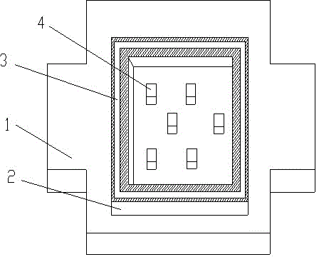
[0014] see figure 1 , the embodiment of the present invention includes:

[0015] A wafer seat, comprising a wafer seat body 1, an annular seat 2 is arranged in the center of the upper end surface of the wafer seat body 1, and the annular seat 2 protrudes from the upper end surface of the wafer seat body 1, and the annular seat 2 Correspondingly, an annular groove 3 is provided, and a plurality of convex sticking points 4 are arranged on the end surface of the crystal seat body between the ring seats 2 .

[0016] In...


PUM


Abstract

The invention discloses a wafer seat which comprises a wafer seat main body, wherein an annular seat is arranged in the middle of the upper end surface of the wafer seat main body and is arranged in a way of projecting the upper end surface of the wafer seat, and an annular groove is correspondingly formed in the wafer seat; a plurality of convex sticking points are arranged on the end surface of the wafer seat main body in the annular seat, and the arrangement height of each convex sticking point is flush with that of the annular seat. By the mode, the wafer seat can increase the adhesion degree between the wafer and the wafer seat and enable redundant tin liquid flowing out during wafer welding to flow along the annular groove so as not to cause overflow.

Description

technical field [0001] The invention relates to the field of wafer processing, in particular to a high-viscosity wafer seat. Background technique [0002] Silicon is a semiconductor material, and its own conductivity is not very good. However, its resistivity can be precisely controlled by adding appropriate dopants. Before semiconductors can be manufactured, silicon must be converted into wafers. Processing silicon wafers to produce an ingot can take anywhere from a week to a month, depending on many factors, including size, quality and end-user requirements. Semiconductors or chips are produced from silicon. Etched into the wafer are millions of transistors hundreds of times smaller than a human hair. Semiconductors manage data by controlling current to form various characters, numbers, sounds, images and colors. They are widely used in integrated circuits and indirectly by everyone on the planet. These applications range from everyday applications such as computers,...

Claims


Application Information

Patent Timeline
Patent Type & Authority Applications(China)
IPC IPC(8): H01L23/13
Inventor 黄根友
Owner WUXI KENUODA ELECTRONICS
Why Eureka
Try Eureka