A method of manufacturing a stepped circuit board

A circuit board manufacturing and ladder technology, applied in the directions of printed circuit manufacturing, printed circuits, printed circuits, etc., can solve the problems of difficult to clean, easy delamination of circuit boards, and difficult removal of gaskets, so as to avoid easy delamination. Effect

Active Publication Date: 2017-10-10
SHENNAN CIRCUITS
View PDF2 Cites 0 Cited by
  • Summary
  • Abstract
  • Description
  • Claims
  • Application Information

AI Technical Summary

Problems solved by technology

[0003] However, the above-mentioned manufacturing method of the stepped circuit board has the following problems: there will be glue flow above the gasket covered at the position of the stepped groove, which makes it difficult to remove the gasket; part of the gasket itself will remain at the bottom of the stepped groove, which is difficult to remove; Covered spacers and tapes during lamination can cause boards to delaminate easily; especially if more than two stepped slots are made, more laminations are required, further delaminating the board

Method used


Image

  • A method of manufacturing a stepped circuit board
  • A method of manufacturing a stepped circuit board
  • A method of manufacturing a stepped circuit board

Examples


Embodiment 1

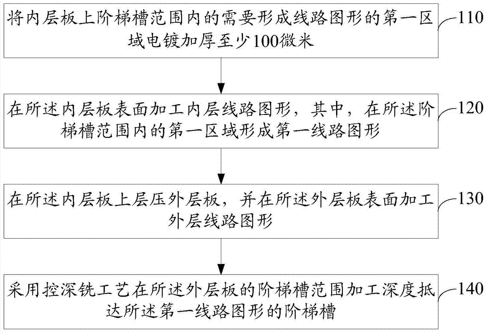
[0016] Please refer to figure 1 , an embodiment of the present invention provides a method for manufacturing a stepped circuit board, including:

[0017] 110. Thicken the first area of ​​the inner layer board where the circuit pattern needs to be formed by electroplating at least 100 microns.

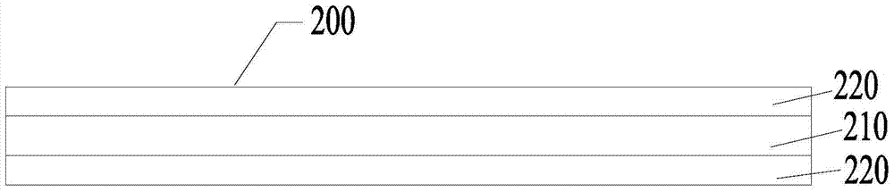
[0018] The inner board can be a double-sided copper-clad board, or a laminated multi-layer board. This article takes double-sided copper clad laminate as an example to illustrate. The bottom of the stepped groove to be formed later will reach the surface of the inner layer board.

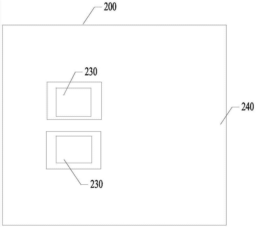
[0019] Such as Figure 2a As shown, the inner board 200 includes a core board layer 210 in the middle and copper foil layers 220 on both sides. Such as Figure 2b As shown, the surface of the inner plate 200 can be divided into two parts, one is the range 230 of the stepped groove, and the other is the range 240 other than the stepped groove.

[0020] In this embodiment, before processing the circuit pa...


PUM


Abstract

The invention discloses a manufacturing method of a step-type circuit board. The manufacturing method comprises the following steps: a first area where a circuit pattern needs to be formed in a step-slot range on an inner-layer board is electrically plated and thickened by at least 100 micrometers; an inner-layer line pattern is machined on the surface of the inner-layer board, wherein a first line pattern is formed in the first area in the step-slot range; an outer-layer board is arranged on an upper layer of the inner-layer board, and an outer-layer line pattern is machined in a surface of the outer-layer board; a step slot with the bottom reaching the first line pattern is machined in step-slot range of the outer-layer board in a depth milling control process. Due to the fact that gaskets do not need to be used in the technical scheme, the problems that the gaskets cannot be removed easily and are left can be avoided, and the problem that layering is likely to occur due to the gaskets can be also avoided; additionally, when multiple step slots need to the machined, all that is needed is to laminate the inner-layer board and the outer-layer board to reach a needed number of layers once and then machine the step slots in the outer-layer board in the depth milling control process, and the problem that layering is likely to occur due to multiple times of lamination can be avoided.

Description

technical field [0001] The invention relates to the technical field of circuit boards, in particular to a method for manufacturing a stepped circuit board. Background technique [0002] For the needs of installing electronic components on the circuit board, etc., it is usually necessary to make stepped grooves on the circuit board. A circuit board with stepped grooves may be called a stepped circuit board. At present, the commonly used method of manufacturing stepped circuit boards includes: first pressing the inner layer where the bottom surface of the stepped groove is located, manually covering the position where the stepped groove needs to be processed on the inner layer surface, and pasting tape on the gasket; and then The outer layer is laminated. After lamination, the groove is opened by controlled depth milling, and the gasket and tape above the stepped groove are exposed and removed by hand, thereby forming a stepped groove. [0003] However, the above-mentioned m...

Claims


Application Information

Patent Timeline
Patent Type & Authority Patents(China)
IPC IPC(8): H05K3/00
CPCH05K3/0014H05K3/4655H05K3/4697H05K2201/09845
Inventor 沙雷刘宝林崔荣
Owner SHENNAN CIRCUITS
Why Eureka
Try Eureka