

Optical detection implantable sensor and manufacturing method and control system thereof
A manufacturing method and sensor technology, applied in the field of medical devices, can solve the problems of complex manufacturing process and high cost, and achieve the effects of simple manufacturing process, small implant trauma, and simple control method
- Summary
- Abstract
- Description
- Claims
- Application Information
AI Technical Summary
Problems solved by technology
Method used
Image

Examples
Embodiment Construction
[0044] The following will clearly and completely describe the technical solutions in the embodiments of the present invention with reference to the accompanying drawings in the embodiments of the present invention. Obviously, the described embodiments are only some of the embodiments of the present invention, not all of them. Based on the embodiments of the present invention, all other embodiments obtained by persons of ordinary skill in the art without making creative efforts belong to the protection scope of the present invention.
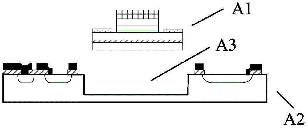
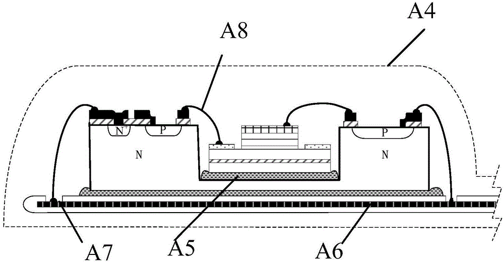
[0045] refer to figure 1 and figure 2 , figure 1 It is a structural schematic diagram of a light detection implantable sensor with a separate structure before packaging, figure 2 It is a schematic structural diagram of a packaged photodetection implantable sensor with a separate structure, and the photodetection implantable sensor with a separate structure includes: a light emitting device A1 and a photosensitive device A2. The light emittin...
PUM
 Abstract
Description
Claims
Application Information