Manufacturing method of circuit board

A manufacturing method and circuit board technology, applied in the direction of printed circuit manufacturing, printed circuits, electrical components, etc., can solve problems such as difficult handling, long process flow, damage to surface tin, etc., to shorten production time, simplify processing flow, and improve production. The effect of efficiency

Active Publication Date: 2015-05-06
NEW FOUNDER HLDG DEV LLC +1
View PDF7 Cites 11 Cited by
  • Summary
  • Abstract
  • Description
  • Claims
  • Application Information

AI Technical Summary

Problems solved by technology

[0003] However, electroplating and filling holes cannot be obtained by alkaline etching. The alkaline etching method is to electroplate first and then plug the hole. After the plug hole is solidified, the grinding process will destroy the surface tin. In the end, it cannot be etched by alkali, and the dry film will also be worn. ; However, steps, edge metallization, and ring-free holes cannot be obtained by acid etching (the dry film sealing ability cannot be guaranteed), so it is more difficult to deal with the coexistence of the two
If the method of alkaline etching is all used, the process will be long, and the surface copper and the hole copper will be plated together, and then the resin will plug the hole, and when the copper is deposited again and the pad of the hole in the plate is electroplated, the surface copper will be too thick to be fine-tuned. line

Method used


Image

  • Manufacturing method of circuit board
  • Manufacturing method of circuit board

Examples


Embodiment Construction

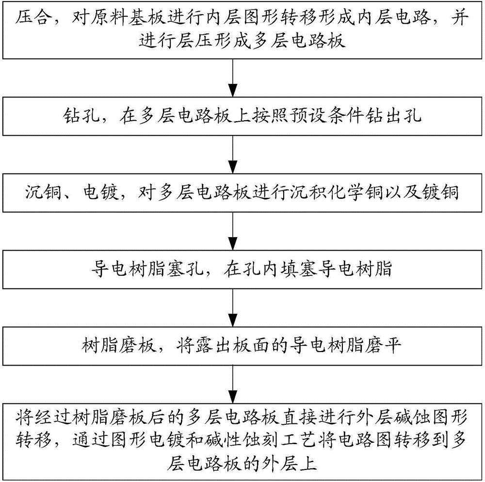
[0031] The structure and principle of the present invention will be described in detail below in conjunction with the accompanying drawings, and the examples given are only used to explain the present invention, not to limit the protection scope of the present invention.

[0032] In the current industry, because POFV (electroplating filling hole) cannot be obtained by alkali etching (alkaline etching, that is, electroplating first and then plugging the hole, the grinding process after the plugging hole is solidified will destroy the surface tin, and finally cannot be alkali-etched, dry The film is also worn), so the circuit board designed for POFV mainly operates in the following ways:

[0033] Lamination→drilling→immersion copper / electroplating→resin plug hole→curing→resin grinding plate→immersion copper / electroplating 2→outer layer acid etching pattern transfer;

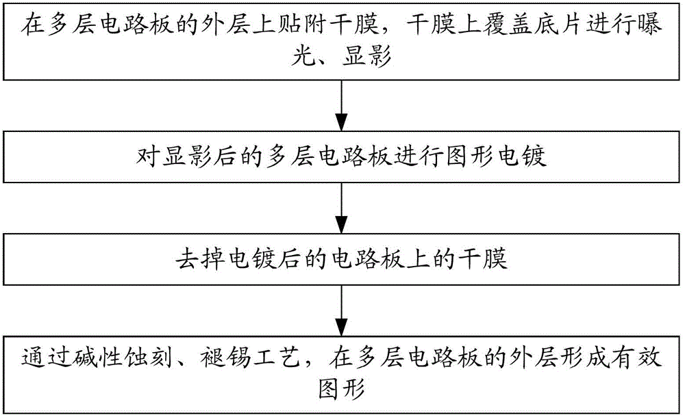
[0034] For the above process, the circuit boards in the industry generally go through the acid etching process a...


PUM


Abstract

The invention relates to a manufacturing method of circuit board; the method comprises the following steps: lamination, applying an inner layer pattern transfer to a raw material substrate to form an inner layer circuit, and laminating to form a multi-layer circuit board; drilling, drilling holes on the multi-layer circuit board based on preset conditions; copper deposition and electroplating, depositing chemical copper and plating copper on the multi-layer circuit board; the method further comprises steps of: blocking holes with conduction resin, filling a conductive resin in the holes; resin grinding, grinding the conductive resin exposed out of the board surface; directly applying outer layer alkali etching pattern transfer to the resin-grinded multi-layer circuit board; transferring the circuit pattern on the outer layer of the multi-layer circuit board by pattern electroplating and alkali etching technology. The manufacturing method of circuit board has the following advantages: the technical limitation that alkali etching process cannot be applied in designing and making the outer layer of the board by POFV (Via Filling Plating) is broken through; copper deposition and electroplating are no longer needed after grinding the resin; the positive pattern transfer can be directly implemented; the machining process of the PCB board can be simplified; the production period is shortened; and the production efficiency is increased.

Description

technical field [0001] The invention relates to the field of circuit board manufacturing, in particular to a method for manufacturing a circuit board. Background technique [0002] With the continuous development of communication products, PCB boards are more and more widely used in high-frequency and high-speed fields, and their designs have also begun to develop towards lightweight, with more and more dense wiring, and the insurmountable popularity of resin plug hole design, even There are a large number of products with special process requirements such as POFV (plated on filled via, electroplating and filling), steps, plate edge metallization, and ring-free holes / slots. [0003] However, electroplating and filling holes cannot be obtained by alkaline etching. The alkaline etching method is to electroplate first and then plug the hole. After the plug hole is solidified, the grinding process will destroy the surface tin. In the end, it cannot be etched by alkali, and the d...

Claims


Application Information

Patent Timeline
Patent Type & Authority Applications(China)
IPC IPC(8): H05K3/00
CPCH05K3/185H05K3/4611
Inventor 罗龙康益平朱兴华陈显任喻恩
Owner NEW FOUNDER HLDG DEV LLC
Why Eureka
Try Eureka