Measuring device, measuring method and application of material micro-area conductance and thermoelectric properties
A measuring method and technology of measuring device, which are applied in the direction of measuring device, measuring electrical variable, measuring resistance/reactance/impedance, etc., and can solve the problems of inability to measure the conductance and thermoelectric potential of material in micro-area.
- Summary
- Abstract
- Description
- Claims
- Application Information
AI Technical Summary
Problems solved by technology
Method used
Image
Examples
Embodiment 1
[0038] Embodiment 1: The conductance of film sample is measured
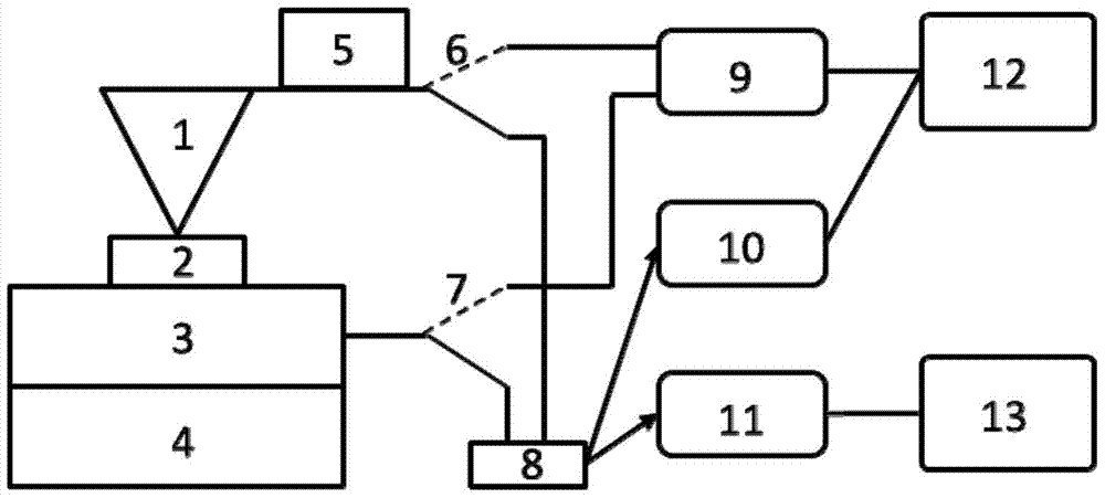
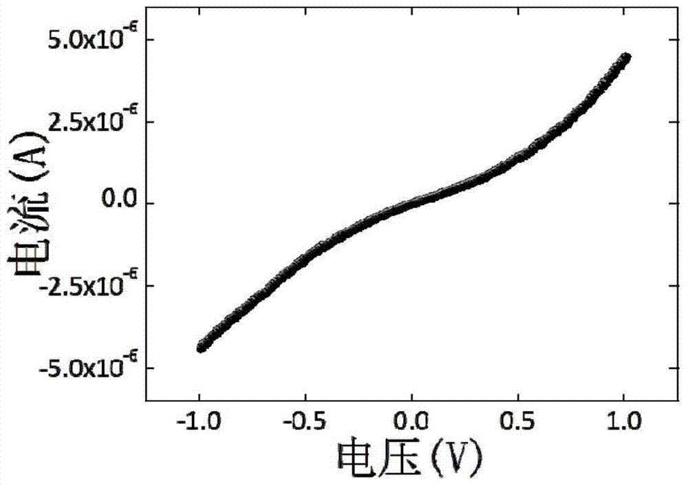
[0039] Such as figure 1As described above, the thin film sample 2 is deposited on the conductive metal substrate 3, the conductive metal substrate 3 is adhered to the temperature control sample stage 4, the conductive probe 1 is in contact with the surface of the thin film sample 2 under the control of the atomic force microscope controller 11, and the thin film sample 2 The conductive metal base 3 below forms two electrodes, and the host computer 12 controls the first static contact of the first relay 6 and the second relay 7 to be in a closed state so that the conductive probe 1 and the conductive metal base 3 are connected to the programmable current source meter 9 connected, the host 12 controls the program-controlled current source meter 9 to output a series of voltages on the conductive probe 1 and the conductive metal substrate 3, and measure the current value returned from the conductive probe 1 and the ...
Embodiment 2
[0040] Embodiment 2: measure the thermoelectric potential of film sample
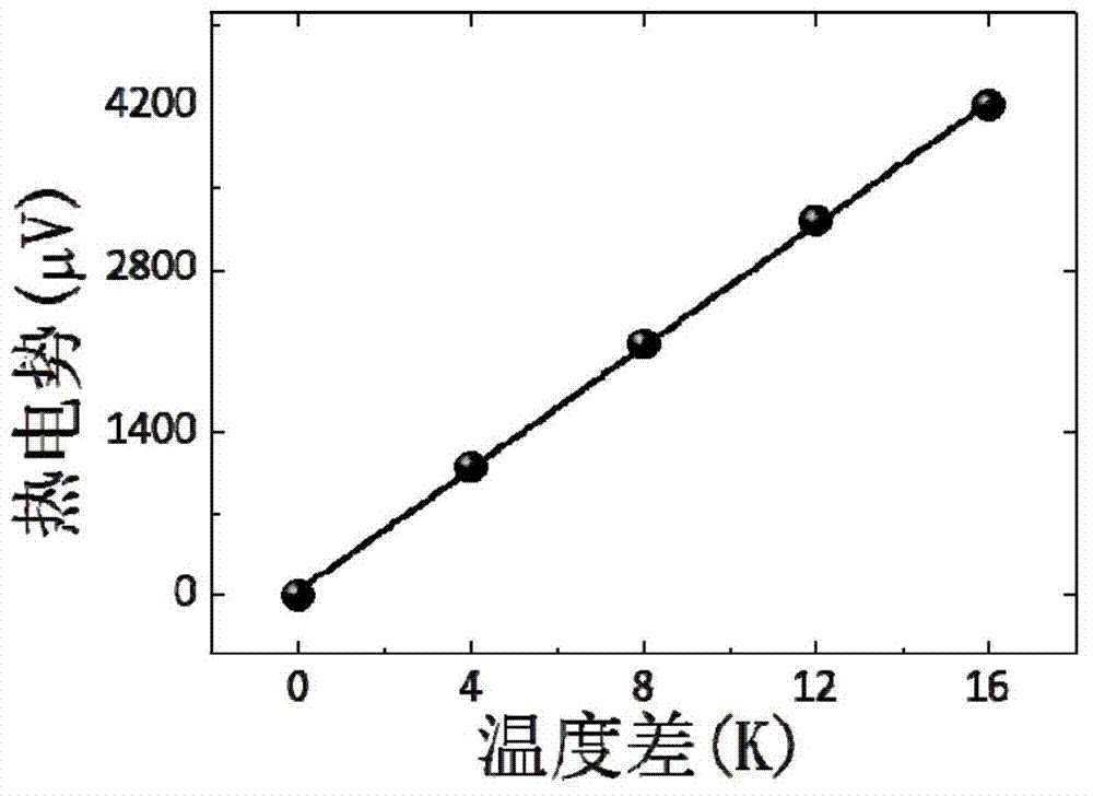
[0041] The thin film sample 2 is deposited on the conductive metal substrate 3, the conductive metal substrate 3 is adhered to the temperature control sample stage 4, the sample 2 to be tested is heated to a known temperature higher than room temperature through the temperature control sample stage 4, and the conductive probe 1 Contact with the film sample 2 surface under the control of the atomic force microscope controller 11, form two electrodes with the conductive metal substrate 3 below the film sample 2, maintain the conductive probe 1 at room temperature through the high thermal conductivity cold storage 5, and conduct the conductive probe 1 A temperature gradient of a micro-region will be generated nearby, and this temperature gradient forms a potential difference between the conductive metal substrate 3 and the conductive probe 1, and the host computer 12 controls the second static contact of th...
Embodiment 3
[0042] Example 3: Simultaneous imaging of thermoelectric potential and sample morphology of thin film samples
[0043] The thin film sample 2 is deposited on the conductive metal substrate 3, the conductive metal substrate 3 is adhered to the temperature control sample stage 4, the sample 2 to be tested is heated to a known temperature higher than room temperature through the temperature control sample stage 4, and the conductive probe 1 Contact with the film sample 2 surface under the control of the atomic force microscope controller 11, form two electrodes with the conductive metal substrate 3 below the film sample 2, maintain the conductive probe 1 at room temperature through the high thermal conductivity cold storage 5, and conduct the conductive probe 1 A temperature gradient of a micro-region will be generated nearby, and this temperature gradient forms a potential difference between the conductive metal substrate 3 and the conductive probe 1, and the host computer 12 con...
PUM
 Abstract
Description
Claims
Application Information
 - R&D Engineer
- R&D Manager
- IP Professional
- Industry Leading Data Capabilities
- Powerful AI technology
- Patent DNA Extraction
Browse by: Latest US Patents, China's latest patents, Technical Efficacy Thesaurus, Application Domain, Technology Topic, Popular Technical Reports.
© 2024 PatSnap. All rights reserved.Legal|Privacy policy|Modern Slavery Act Transparency Statement|Sitemap|About US| Contact US: help@patsnap.com


