A surface treatment method for a light-absorbing layer of a kesterite-structured thin-film solar cell
A technology for solar cells and light-absorbing layers, applied in the field of solar cells, can solve problems such as high defect density, affect the photoelectric conversion efficiency of solar cells, and mismatch of p-n junction energy levels, achieve passivation of interface defects, overcome surface defects, and improve Effect of open circuit voltage and fill factor
- Summary
- Abstract
- Description
- Claims
- Application Information
AI Technical Summary
Problems solved by technology
Method used
Image
Examples
Embodiment 1
[0024] Preparation of kesterite structure thin film solar cell light absorbing layer Cu 2 CdGeSe 4 Afterwards, the sample was first mixed with 0.1mol / L Na + , 0.7mol / L Ca 2+ and 0.5mol / L Fe 3+ Soak in a metal salt solution (solution temperature 10°C, immersion time 3.5h), and then keep it in a nitrogen atmosphere at 150°C for 90 minutes, and finally prepare a device.
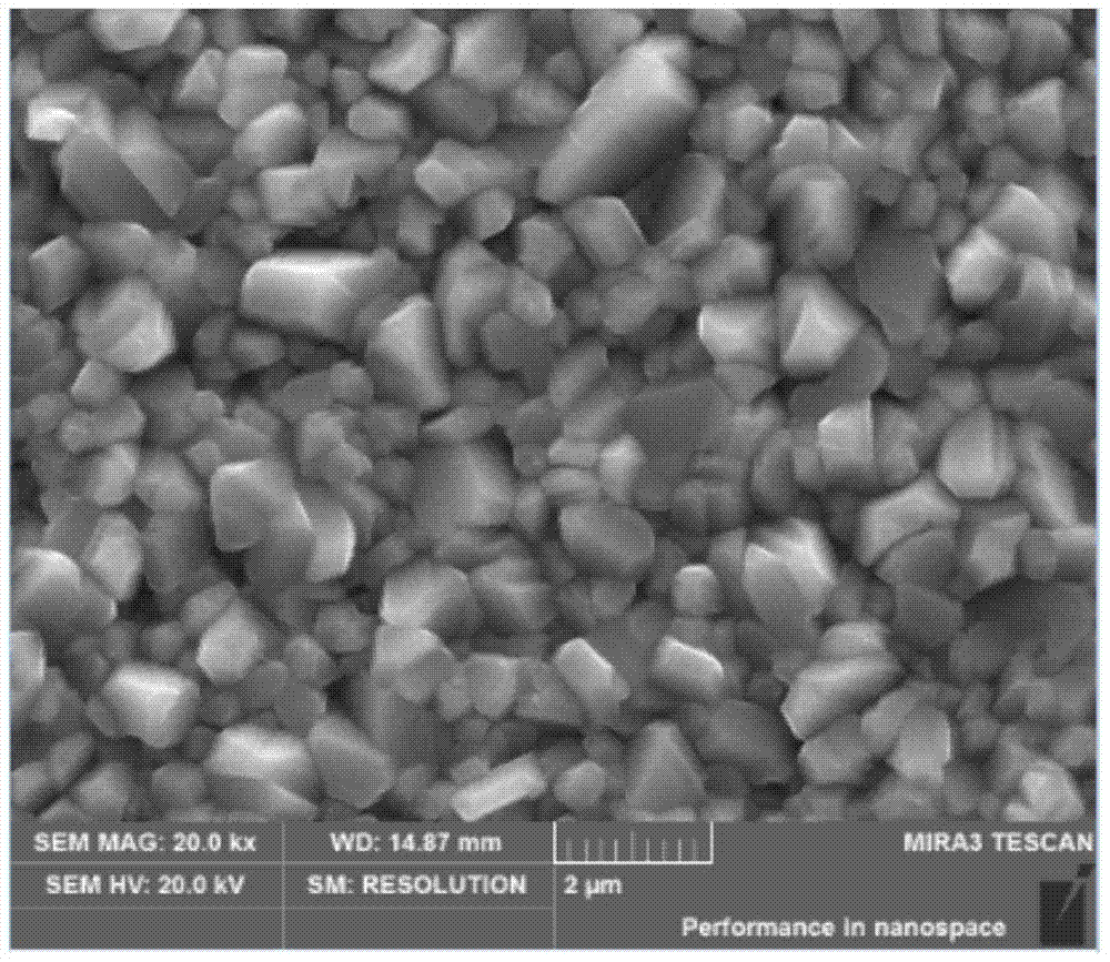
[0025] Prepared Cu 2 CdGeSe 4 The open circuit voltage of the thin film solar cell is 403mV, and the short circuit current density is 26.98mA / cm 2 , the fill factor is 48%, and the photoelectric conversion efficiency of the cell is 5.22%. Such as figure 1 Shown is the SEM image of the surface after ion immersion treatment, by figure 1 It can be seen that the surface morphology is dense and smooth, the grain size is large, and there are no obvious holes or defects.
Embodiment 2
[0027] Preparation of kesterite structure thin film solar cell light absorbing layer Cu 2 ZnSnS 4 Afterwards, the sample was first mixed with 0.3mol / LK + , 0.5mol / LAg + , 0.6mol / LMg 2+ , 0.5mol / LCu 2+ , 0.4mol / LZn 2+ , 0.4mol / LCr 3+ Soak in a metal salt solution (solution temperature 30°C, immersion time 2.5h), and then keep it in an argon atmosphere at 250°C for 70 minutes, and finally prepare a device.
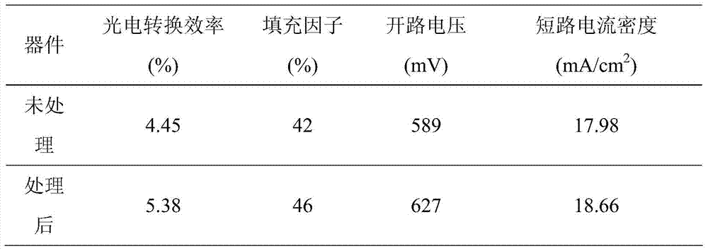
[0028] The performance of the device without immersion annealing process is shown in Table 1. It can be seen from the table that the open circuit voltage, fill factor and photoelectric conversion efficiency of the device after the treatment have been improved to a certain extent.
[0029] Table 1 device performance comparison
[0030]
Embodiment 3
[0032] Preparation of kesterite structure thin film solar cell light absorbing layer Ag 4 CdG 4 Afterwards, the sample was first mixed with 0.3mol / L In 3+ soaked in a metal salt solution (solution temperature 50°C, soaking time 2h), and then kept at 350°C for 50 minutes under a sulfur vapor atmosphere, and finally prepared into a device.
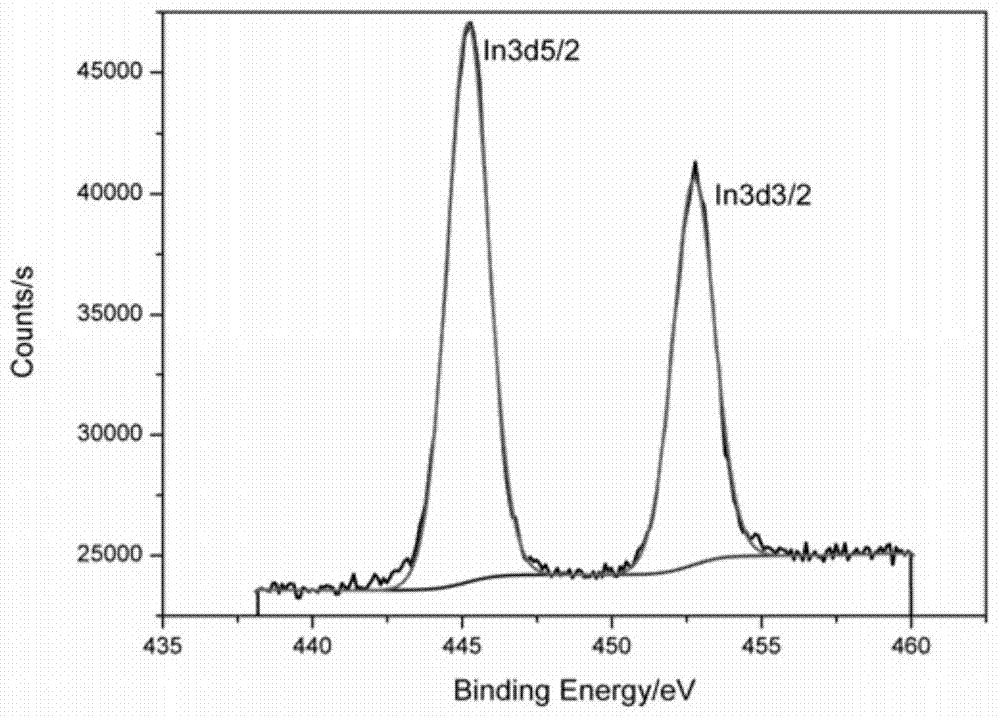
[0033] Prepared Ag 4 CdG 4 The open circuit voltage of the thin film solar cell is 615mV, and the short circuit current density is 17.74mA / cm 2 , the fill factor is 47%, and the photoelectric conversion efficiency of the cell is 5.13%. Such as figure 2 As shown, it is the fitting curve of In element under XPS detection. It can be seen from the detection results that the effective doping and incorporation of metal elements can be realized by soaking.
PUM
 Abstract
Description
Claims
Application Information


